High-Vacuum Technique Integration with Computational Lithography
APR 24, 20269 MIN READ
Generate Your Research Report Instantly with AI Agent
Patsnap Eureka helps you evaluate technical feasibility & market potential.
High-Vacuum Lithography Background and Technical Objectives
High-vacuum lithography represents a critical convergence of precision manufacturing and advanced computational modeling, emerging as a cornerstone technology for next-generation semiconductor fabrication. This integration addresses the fundamental limitations of conventional atmospheric lithography processes, where particle contamination and atmospheric interference significantly constrain pattern resolution and fidelity. The evolution from traditional photolithography to high-vacuum computational lithography reflects the industry's response to Moore's Law scaling challenges and the demand for sub-10nm feature geometries.
The historical development of this technology traces back to early electron beam lithography systems in the 1960s, which first demonstrated the advantages of vacuum environments for precision patterning. However, the integration with computational lithography emerged prominently in the 2000s as semiconductor manufacturers encountered resolution limits with conventional optical systems. The synergy between vacuum processing and computational correction algorithms has enabled breakthrough achievements in pattern accuracy and defect reduction.
Contemporary high-vacuum lithography systems operate under ultra-high vacuum conditions, typically maintaining pressures below 10^-8 Torr to eliminate molecular contamination and scattering effects. The computational component encompasses sophisticated algorithms for proximity effect correction, dose modulation, and real-time pattern optimization. This dual approach addresses both physical and computational barriers to achieving atomic-scale precision in semiconductor manufacturing.
The primary technical objectives center on achieving sub-5nm critical dimension control while maintaining throughput compatibility with industrial production requirements. Key performance targets include reducing line edge roughness to below 1nm, achieving overlay accuracy within 0.5nm tolerances, and minimizing defect densities to fewer than 0.01 defects per square centimeter. Additionally, the integration aims to enable three-dimensional patterning capabilities for advanced device architectures.
Process optimization objectives focus on developing predictive models that can anticipate and compensate for vacuum-induced effects, thermal variations, and substrate interactions. The computational framework must accommodate real-time feedback mechanisms, enabling dynamic adjustment of exposure parameters based on in-situ monitoring data. This closed-loop approach represents a paradigm shift toward intelligent manufacturing systems capable of autonomous quality control and process optimization.
Market Demand for Advanced Semiconductor Manufacturing
The semiconductor manufacturing industry is experiencing unprecedented demand driven by the proliferation of artificial intelligence, high-performance computing, and advanced mobile technologies. This surge has created an urgent need for more sophisticated manufacturing processes capable of producing chips with smaller geometries and higher performance specifications. The integration of high-vacuum techniques with computational lithography represents a critical technological convergence addressing these market pressures.
Advanced semiconductor nodes below 7nm require extreme precision in manufacturing processes, where traditional lithography approaches face fundamental physical limitations. The market demand for these cutting-edge semiconductors spans multiple sectors, including data centers requiring AI accelerators, automotive applications demanding advanced driver assistance systems, and consumer electronics pushing for enhanced processing capabilities. Each sector requires chips with specific performance characteristics that can only be achieved through advanced manufacturing techniques.
The computational lithography market segment has emerged as a vital component in addressing resolution enhancement and process optimization challenges. Manufacturers are increasingly seeking solutions that combine high-vacuum environments with sophisticated computational modeling to achieve the precision required for next-generation semiconductor devices. This demand is particularly acute in the production of logic processors, memory devices, and specialized chips for emerging applications.
Market dynamics indicate a strong preference for manufacturing solutions that can simultaneously improve yield rates, reduce defect densities, and enable smaller feature sizes. The integration of high-vacuum techniques with computational lithography directly addresses these requirements by providing enhanced process control and predictive capabilities. This technological combination enables manufacturers to optimize exposure conditions, minimize contamination effects, and achieve better pattern fidelity.
The economic drivers supporting this market demand include the substantial capital investments required for advanced semiconductor fabrication facilities and the need to maximize return on these investments through improved manufacturing efficiency. Companies are actively seeking technologies that can extend the capabilities of existing lithography equipment while preparing for future node requirements, making the integration of high-vacuum techniques with computational lithography a strategically important market opportunity.
Current State of High-Vacuum Computational Lithography
High-vacuum computational lithography represents a convergence of advanced vacuum technology and sophisticated computational modeling techniques, currently experiencing rapid development across multiple technological fronts. The integration combines ultra-high vacuum environments, typically operating at pressures below 10^-9 Torr, with real-time computational algorithms to optimize lithographic processes for next-generation semiconductor manufacturing.
Leading semiconductor manufacturers including TSMC, Samsung, and Intel have established comprehensive high-vacuum computational lithography capabilities within their advanced fabrication facilities. These implementations primarily focus on extreme ultraviolet (EUV) lithography systems, where vacuum conditions are critical for preventing photon absorption and maintaining pattern fidelity. The computational components utilize machine learning algorithms and physics-based models to predict and compensate for vacuum-related distortions in real-time.
Current technological implementations demonstrate significant variations in approach and maturity levels. ASML's EUV systems incorporate vacuum-integrated computational correction algorithms that achieve sub-nanometer precision in pattern placement. These systems employ distributed computing architectures that process vacuum sensor data, thermal measurements, and optical feedback simultaneously to maintain optimal lithographic conditions.
The primary technical challenges center around maintaining computational accuracy under extreme vacuum conditions while managing the complex interactions between vacuum dynamics and lithographic precision. Outgassing from computational hardware components introduces contamination risks that can compromise both vacuum integrity and pattern quality. Additionally, the electromagnetic interference generated by high-performance computing systems can affect sensitive vacuum measurement instruments and lithographic alignment systems.
Geographically, the most advanced high-vacuum computational lithography capabilities are concentrated in East Asia, particularly in Taiwan, South Korea, and Japan, where major semiconductor foundries have invested heavily in integrated vacuum-computational infrastructure. European research institutions, notably IMEC in Belgium, have developed innovative approaches focusing on hybrid vacuum-atmospheric computational modeling techniques.
Recent technological breakthroughs include the development of vacuum-compatible edge computing modules that can operate directly within lithographic chambers, reducing latency in computational feedback loops. These systems utilize specialized radiation-hardened processors and custom cooling solutions designed for ultra-high vacuum environments, enabling real-time optimization of lithographic parameters based on instantaneous vacuum conditions and computational predictions.
Existing High-Vacuum Computational Lithography Solutions
01 Computational lithography for mask optimization and pattern correction
Advanced computational lithography techniques are employed to optimize photomask designs and correct optical proximity effects in semiconductor manufacturing. These methods utilize algorithms and simulation models to predict and compensate for distortions that occur during the lithography process, enabling more accurate pattern transfer at nanoscale dimensions. The computational approaches include optical proximity correction, inverse lithography technology, and source-mask optimization to enhance resolution and pattern fidelity.- Computational lithography for mask optimization and OPC: Computational lithography techniques are employed to optimize photomask designs and perform optical proximity correction (OPC). These methods use advanced algorithms and simulation models to predict and compensate for optical effects during the lithography process, improving pattern fidelity and resolution. The computational approaches enable precise control over feature dimensions and placement, accounting for diffraction, interference, and other optical phenomena that occur during exposure.
- High-vacuum systems for lithography equipment: High-vacuum technology is integrated into lithography systems to maintain ultra-clean environments during the exposure and patterning processes. Vacuum systems prevent contamination and enable precise control of the atmospheric conditions within the lithography chamber. These systems are critical for advanced semiconductor manufacturing, where even minute particles can cause defects. The vacuum environment also facilitates the use of certain exposure wavelengths and enables better control of thermal conditions during processing.
- Integration of metrology and inspection systems with computational models: Advanced metrology and inspection systems are integrated with computational lithography frameworks to provide real-time feedback and process control. These systems measure critical dimensions, overlay accuracy, and defect detection, feeding data back into computational models for continuous optimization. The integration enables closed-loop control where measurement data directly influences subsequent lithography steps, improving yield and reducing process variations.
- Multi-patterning techniques with computational assistance: Multi-patterning lithography approaches utilize computational methods to decompose complex patterns into multiple simpler exposures. These techniques are essential for achieving feature sizes below the optical resolution limit. Computational algorithms determine optimal pattern splitting strategies, assign features to different mask layers, and minimize conflicts between exposures. The integration of vacuum processing ensures precise alignment and minimal contamination between successive patterning steps.
- Source-mask optimization and illumination control: Source-mask optimization (SMO) techniques jointly optimize the illumination source and mask patterns using computational algorithms. These methods determine optimal pupil shapes, polarization states, and intensity distributions to maximize imaging performance. The computational optimization considers the entire optical system including vacuum chamber conditions and enables the achievement of enhanced resolution and process windows. Advanced algorithms balance multiple objectives including contrast, depth of focus, and manufacturing constraints.
02 High-vacuum deposition systems for lithography applications
High-vacuum techniques are integrated into lithography processes to enable precise material deposition and pattern formation in controlled environments. These systems maintain ultra-low pressure conditions to minimize contamination and ensure high-quality thin film deposition for semiconductor device fabrication. The vacuum environment is critical for processes such as electron beam lithography, ion beam lithography, and advanced photoresist processing where atmospheric interference must be eliminated.Expand Specific Solutions03 Integrated metrology and process control in vacuum lithography systems
Real-time monitoring and control systems are incorporated into high-vacuum lithography equipment to ensure process stability and pattern accuracy. These integrated metrology solutions provide feedback mechanisms for adjusting exposure parameters, alignment precision, and environmental conditions during the lithography process. The combination of in-situ measurement capabilities with computational models enables adaptive process control and defect reduction.Expand Specific Solutions04 Multi-patterning techniques with computational design optimization
Multiple exposure and patterning strategies are combined with computational design methods to achieve feature sizes beyond the diffraction limit of lithography systems. These techniques involve decomposing complex patterns into multiple simpler masks that are sequentially processed, with computational algorithms determining optimal pattern splits and overlay strategies. The integration of simulation tools helps predict and mitigate potential defects arising from the multi-step patterning process.Expand Specific Solutions05 Extreme ultraviolet lithography with vacuum environment integration
Extreme ultraviolet lithography systems operate in high-vacuum conditions due to the strong absorption of EUV radiation by atmospheric gases. The integration of computational lithography with EUV technology requires specialized vacuum chambers, reflective optics, and contamination control mechanisms. Computational models are essential for optimizing mask designs, correcting for flare effects, and managing the unique challenges of EUV pattern transfer in vacuum environments.Expand Specific Solutions
Key Players in High-Vacuum Lithography Equipment Industry
The high-vacuum technique integration with computational lithography represents a mature yet rapidly evolving technological domain, currently in an advanced development stage driven by semiconductor industry demands for sub-nanometer precision manufacturing. The market demonstrates substantial scale, exceeding billions in annual investment, primarily concentrated among established players like ASML Netherlands BV and Carl Zeiss SMT GmbH who dominate lithography equipment manufacturing. Technology maturity varies significantly across participants: industry leaders such as Taiwan Semiconductor Manufacturing Co., Intel Corp., and GlobalFoundries U.S. Inc. demonstrate production-ready implementations, while companies like Synopsys Inc. and Cadence Design Systems Inc. provide essential computational infrastructure. Research institutions including Beijing Institute of Technology, Xidian University, and Interuniversitair Micro-Electronica Centrum VZW contribute foundational innovations. Emerging players like D2S Inc. and Hermes Microvision Inc. focus on specialized e-beam solutions, indicating continued technological advancement and market expansion opportunities.
ASML Netherlands BV
Technical Solution: ASML integrates advanced high-vacuum systems with computational lithography in their extreme ultraviolet (EUV) lithography machines. Their technology combines ultra-high vacuum chambers operating at 10^-9 torr levels with sophisticated computational correction algorithms to enable sub-7nm semiconductor manufacturing. The vacuum system maintains contamination-free environments essential for EUV mirror reflectivity, while computational lithography algorithms correct for optical proximity effects, mask errors, and process variations in real-time during exposure.
Strengths: Market leader in EUV lithography with proven high-vacuum integration, advanced computational correction capabilities. Weaknesses: Extremely high system costs, complex maintenance requirements, limited throughput compared to traditional lithography.
International Business Machines Corp.
Technical Solution: IBM develops computational lithography solutions that integrate with high-vacuum processing environments for advanced semiconductor manufacturing. Their approach focuses on machine learning-enhanced optical proximity correction (OPC) and source mask optimization (SMO) algorithms that operate within vacuum-based lithography systems. IBM's technology emphasizes curvilinear mask designs and advanced computational models that account for vacuum-specific optical effects and contamination control requirements in next-generation lithography processes.
Strengths: Strong computational expertise, advanced AI/ML integration in lithography algorithms, extensive semiconductor manufacturing experience. Weaknesses: Limited direct equipment manufacturing capabilities, dependency on partnerships for vacuum system integration.
Core Patents in Vacuum-Computational Lithography Integration
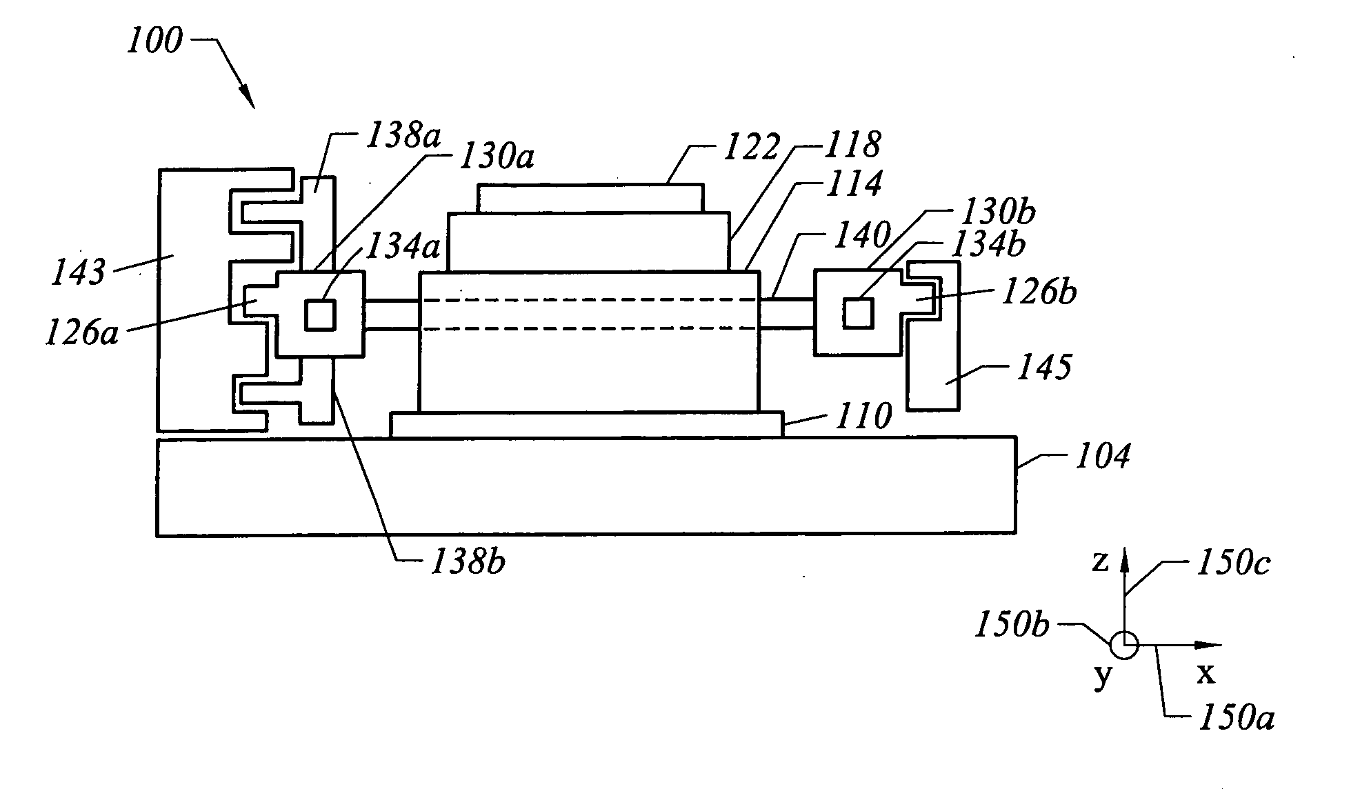
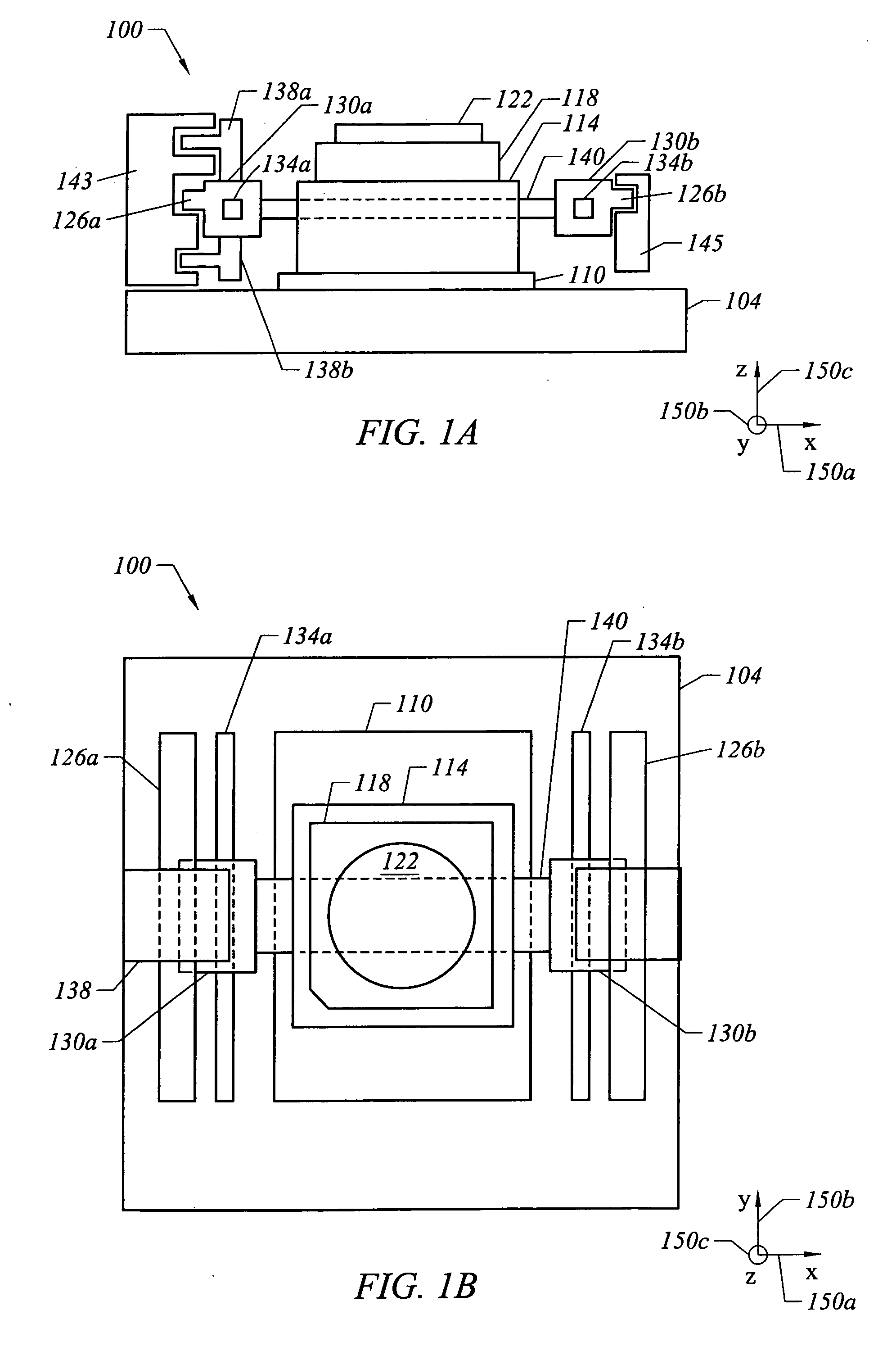
Wafer stage operable in a vacuum environment
PatentInactiveUS20050168076A1
Innovation
- A stage apparatus with vacuum-compatible air bearings and a levitating fine stage, supported by electromagnetic actuators, which allows for precise scanning of objects in a vacuum environment without significant gas leakage or thermal compromise, using grooves for vacuum and pressurized gas management and electromagnetic support for six degrees of freedom.
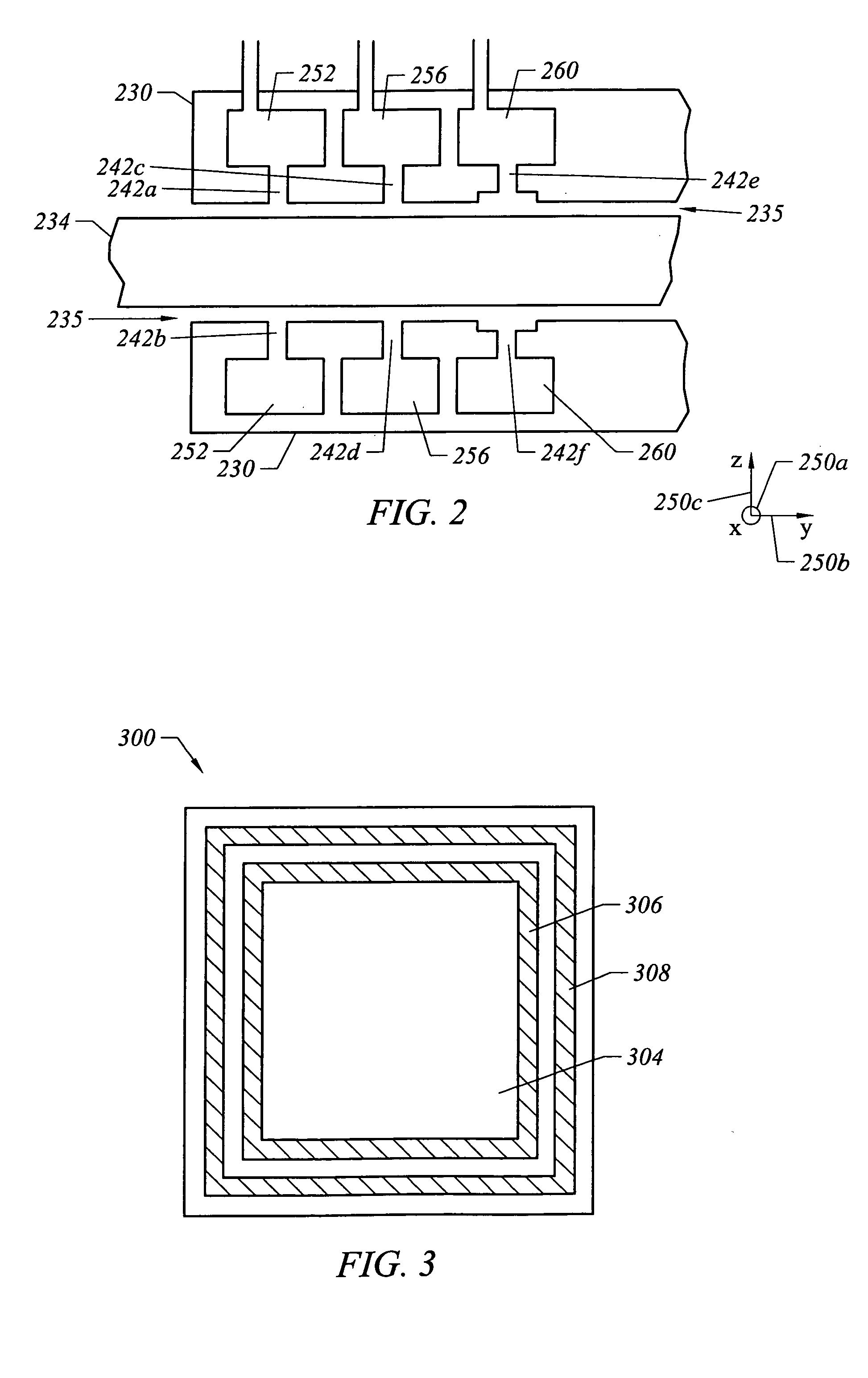

Apparatus for and method of thermophoretic protection of an object in a high-vacuum environment
PatentInactiveUS7745079B2
Innovation
- A particle deposition reduction system using a chamber with a shielding plate and gas ports to emit high-pressure gas parallel to the reticle surface, creating a temperature gradient that accelerates particles away from the surface, while maintaining a low conductance seal to prevent gas flow and ensure thermophoretic protection in a high vacuum environment.


Environmental and Safety Standards for Vacuum Systems
The integration of high-vacuum techniques with computational lithography necessitates stringent environmental and safety standards to ensure operational integrity and personnel protection. These standards encompass multiple regulatory frameworks, including ISO 14040 series for environmental management, OSHA guidelines for workplace safety, and semiconductor industry-specific protocols such as SEMI S2 and S8 standards.
Vacuum systems operating in lithography environments must comply with strict contamination control requirements. Particulate levels must be maintained below 0.1 particles per cubic foot for particles larger than 0.1 micrometers. Chemical contamination limits are equally critical, with molecular airborne contamination levels restricted to parts-per-billion ranges for organic compounds and metallic impurities.
Safety protocols for high-vacuum systems focus on multiple hazard categories. Implosion risks require robust chamber design with safety factors exceeding 4:1 for ultimate vacuum conditions. Electrical safety measures include proper grounding systems, arc flash protection, and fail-safe interlocks preventing operation under unsafe conditions. Personnel must receive specialized training in vacuum safety procedures and emergency response protocols.
Environmental standards address both operational emissions and waste management. Vacuum pump exhaust systems require filtration to prevent release of process chemicals and particulates. Spent pump oils and contaminated components must be handled according to hazardous waste regulations. Energy efficiency standards mandate power consumption optimization and heat recovery systems where applicable.
Gas handling safety represents a critical aspect, particularly for process gases used in computational lithography applications. Toxic and flammable gas detection systems must provide continuous monitoring with automatic shutdown capabilities. Ventilation systems require redundant operation to maintain safe atmospheric conditions during both normal operation and emergency scenarios.
Regular compliance auditing ensures adherence to evolving standards. Documentation requirements include maintenance logs, calibration records, and incident reporting systems. Third-party certification processes validate system compliance and provide ongoing monitoring frameworks for sustained operational safety and environmental protection.
Cost-Benefit Analysis of High-Vacuum Lithography Implementation
The implementation of high-vacuum lithography systems integrated with computational techniques presents a complex investment scenario requiring comprehensive financial evaluation. Initial capital expenditure represents the most significant cost component, encompassing specialized vacuum chambers, precision pumping systems, and advanced computational hardware capable of real-time process modeling. These systems typically require investments ranging from $50-150 million for state-of-the-art facilities, depending on throughput requirements and technology nodes targeted.
Operational expenditures constitute another substantial cost factor, including energy consumption for maintaining ultra-high vacuum conditions, specialized maintenance protocols, and skilled personnel training. High-vacuum systems consume approximately 30-40% more energy than conventional atmospheric lithography processes, while requiring continuous monitoring and predictive maintenance enabled by computational algorithms. The integration of machine learning models for process optimization adds computational infrastructure costs but significantly reduces material waste and rework expenses.
The primary economic benefits emerge through enhanced yield rates and reduced defect densities. High-vacuum environments eliminate atmospheric contaminants that cause critical dimension variations and pattern distortions, particularly crucial for sub-7nm technology nodes. Computational lithography integration enables real-time process corrections, achieving yield improvements of 15-25% compared to conventional systems. This translates to substantial cost savings in high-value semiconductor manufacturing, where single wafer values can exceed $10,000.
Return on investment calculations demonstrate favorable outcomes for high-volume manufacturing scenarios. The break-even point typically occurs within 18-24 months for facilities processing over 10,000 wafers monthly. Long-term benefits include extended equipment lifespan due to reduced contamination-related wear, lower consumable costs through optimized process parameters, and enhanced capability to manufacture next-generation devices that command premium pricing.
Risk mitigation through computational modeling reduces the probability of costly process failures and enables predictive maintenance scheduling, further improving the overall cost-benefit ratio. The technology's scalability across multiple product lines provides additional economic advantages through shared infrastructure utilization and cross-platform process optimization capabilities.
Unlock deeper insights with Patsnap Eureka Quick Research — get a full tech report to explore trends and direct your research. Try now!
Generate Your Research Report Instantly with AI Agent
Supercharge your innovation with Patsnap Eureka AI Agent Platform!