How Piezoelectric Sensors Can Drive Nanopositioning Techniques
JUL 17, 20259 MIN READ
Generate Your Research Report Instantly with AI Agent
Patsnap Eureka helps you evaluate technical feasibility & market potential.
Piezoelectric Nanopositioning Background and Objectives
Piezoelectric nanopositioning represents a cutting-edge technology that has revolutionized precision control in various scientific and industrial applications. The field has evolved significantly over the past few decades, driven by the increasing demand for ultra-precise positioning in areas such as microscopy, semiconductor manufacturing, and nanotechnology.
The fundamental principle behind piezoelectric nanopositioning lies in the unique properties of piezoelectric materials, which deform when subjected to an electric field. This deformation, though minuscule, can be harnessed to achieve positioning accuracies on the nanometer scale. The development of this technology can be traced back to the discovery of the piezoelectric effect by Jacques and Pierre Curie in 1880, but its practical application in nanopositioning only gained momentum in the late 20th century.
As the field progressed, researchers and engineers focused on overcoming key challenges such as hysteresis, creep, and thermal drift, which initially limited the precision and reliability of piezoelectric actuators. Advances in materials science, control systems, and sensor technologies have played crucial roles in addressing these issues and pushing the boundaries of nanopositioning capabilities.
The primary objective of piezoelectric nanopositioning technology is to achieve precise, repeatable, and stable positioning at the nanoscale. This involves not only the development of high-performance actuators but also the integration of sophisticated feedback systems and control algorithms. The ultimate goal is to enable positioning resolutions in the sub-nanometer range while maintaining large travel ranges and high speeds.
In recent years, the focus has shifted towards multi-axis nanopositioning systems, capable of precise movement in three or more degrees of freedom. This advancement has opened up new possibilities in fields such as 3D nanofabrication, high-resolution imaging, and nanometrology. Additionally, there is a growing emphasis on developing compact, energy-efficient nanopositioning systems for portable and space-constrained applications.
The evolution of piezoelectric nanopositioning technology is closely intertwined with advancements in related fields, such as MEMS (Micro-Electro-Mechanical Systems) and nanotechnology. As these disciplines continue to progress, they drive further innovations in nanopositioning techniques, creating a symbiotic relationship that propels the entire field forward.
Looking ahead, the objectives for piezoelectric nanopositioning technology include enhancing long-term stability, increasing positioning speed without compromising accuracy, and developing more robust systems capable of operating in challenging environments. There is also a growing interest in integrating artificial intelligence and machine learning algorithms to optimize nanopositioning performance and adaptability.
Market Analysis for Nanopositioning Technologies
The nanopositioning technologies market has been experiencing significant growth due to increasing demand for high-precision positioning systems across various industries. This market is primarily driven by applications in semiconductor manufacturing, optical systems, microscopy, and advanced scientific research. The global nanopositioning market was valued at approximately $90 million in 2020 and is projected to reach $150 million by 2025, growing at a CAGR of 10.8% during the forecast period.
Piezoelectric sensors play a crucial role in driving nanopositioning techniques, offering several advantages over traditional positioning methods. These sensors provide high resolution, fast response times, and excellent repeatability, making them ideal for nanoscale positioning applications. The integration of piezoelectric sensors in nanopositioning systems has led to improved performance and expanded capabilities in various fields.
In the semiconductor industry, nanopositioning technologies are essential for advanced lithography processes, wafer inspection, and metrology. The increasing demand for smaller and more complex semiconductor devices is driving the adoption of high-precision nanopositioning systems. The automotive sector is also emerging as a significant market for nanopositioning technologies, particularly in the development of advanced driver assistance systems (ADAS) and autonomous vehicles.
The medical and life sciences sectors represent another growing market for nanopositioning technologies. Applications include high-resolution imaging, drug discovery, and precision surgery. The ability of piezoelectric sensor-driven nanopositioning systems to achieve sub-nanometer resolution has opened up new possibilities in these fields.
Geographically, North America and Europe currently dominate the nanopositioning market, accounting for over 60% of the global market share. However, the Asia-Pacific region is expected to witness the highest growth rate in the coming years, driven by rapid industrialization and increasing investments in research and development activities.
Key market players in the nanopositioning technologies sector include Physik Instrumente (PI) GmbH & Co. KG, Mad City Labs Inc., Aerotech Inc., and Piezosystem Jena GmbH. These companies are focusing on developing innovative products and expanding their global presence through strategic partnerships and acquisitions.
Challenges in the market include the high cost of nanopositioning systems and the need for specialized expertise in their operation and maintenance. However, ongoing technological advancements and increasing awareness of the benefits of nanopositioning technologies are expected to drive market growth in the coming years.
Current Challenges in Piezoelectric Nanopositioning
Piezoelectric nanopositioning systems face several significant challenges that hinder their widespread adoption and optimal performance. One of the primary issues is the inherent nonlinearity of piezoelectric materials, which leads to hysteresis and creep effects. These nonlinear behaviors result in positioning inaccuracies and reduced repeatability, particularly in high-precision applications.
Another major challenge is the limited range of motion achievable with piezoelectric actuators. While they excel in providing sub-nanometer resolution, their typical displacement range is restricted to a few tens of micrometers. This limitation constrains their applicability in scenarios requiring both high precision and extended travel ranges.
Thermal drift poses a substantial obstacle to long-term stability in piezoelectric nanopositioning systems. Temperature fluctuations can cause dimensional changes in the piezoelectric elements and surrounding structures, leading to undesired positional shifts. This thermal sensitivity necessitates sophisticated compensation mechanisms or stringent environmental control.
The dynamic performance of piezoelectric nanopositioners is often compromised by mechanical resonances. These resonances can limit the bandwidth of the positioning system and introduce unwanted vibrations, affecting both speed and accuracy. Overcoming these dynamic limitations requires advanced control strategies and mechanical design optimizations.
Cross-coupling between multiple axes in multi-degree-of-freedom nanopositioning systems presents another significant challenge. Movement along one axis can induce unintended motion in other axes, complicating precise positioning tasks. Mitigating this cross-talk effect demands complex calibration procedures and advanced control algorithms.
The integration of sensors for closed-loop feedback control introduces its own set of challenges. While essential for improving accuracy and repeatability, sensors can add complexity, cost, and potential noise sources to the system. Achieving high-resolution sensing without compromising the overall system performance remains a critical area of development.
Lastly, the high voltage requirements of piezoelectric actuators present both safety concerns and design challenges. The need for compact, high-voltage amplifiers that can deliver precise, low-noise signals while maintaining efficiency is an ongoing area of research and development in the field of piezoelectric nanopositioning.
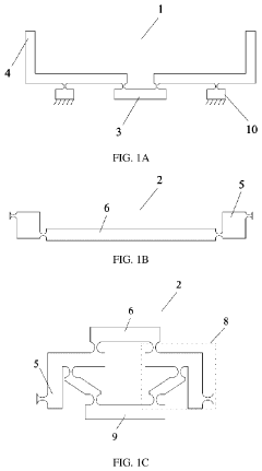
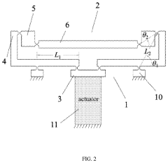
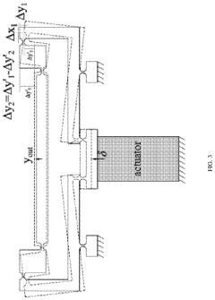
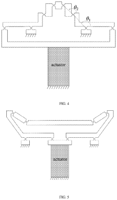
Existing Piezoelectric Nanopositioning Solutions
01 Piezoelectric actuators for nanopositioning
Piezoelectric actuators are used in nanopositioning systems to achieve precise and controlled movements at the nanoscale. These actuators convert electrical energy into mechanical displacement, allowing for high-resolution positioning in various applications such as microscopy, lithography, and precision manufacturing.- Piezoelectric actuators for nanopositioning: Piezoelectric actuators are used in nanopositioning systems to achieve precise and controlled movements at the nanoscale. These actuators convert electrical energy into mechanical motion, allowing for high-resolution positioning in various applications such as microscopy, lithography, and data storage.
- Sensor integration in nanopositioning systems: Integrating sensors into nanopositioning systems enables closed-loop control and improved accuracy. These sensors can measure displacement, force, or other parameters to provide feedback for precise positioning. Various sensor types, including capacitive and optical sensors, are used in conjunction with piezoelectric actuators.
- Multi-axis nanopositioning systems: Multi-axis nanopositioning systems utilize multiple piezoelectric actuators and sensors to achieve precise positioning in multiple directions. These systems can provide movement in X, Y, and Z axes, as well as rotational degrees of freedom, enabling complex nanoscale manipulations for advanced applications.
- Piezoelectric materials for nanopositioning: Advanced piezoelectric materials are developed to enhance the performance of nanopositioning systems. These materials exhibit improved electromechanical properties, such as higher strain coefficients and reduced hysteresis, leading to better positioning accuracy and faster response times in nanoscale applications.
- Control algorithms for nanopositioning: Sophisticated control algorithms are implemented to optimize the performance of piezoelectric nanopositioning systems. These algorithms compensate for nonlinearities, hysteresis, and creep effects inherent in piezoelectric actuators, ensuring high-precision positioning and improved dynamic behavior in nanoscale applications.
02 Sensor integration in nanopositioning systems
Integrating sensors into nanopositioning systems enables closed-loop control and improved accuracy. These sensors can measure displacement, force, or other parameters to provide feedback for precise positioning. Various sensor types, including capacitive and optical sensors, are used in conjunction with piezoelectric actuators to achieve nanometer-level precision.Expand Specific Solutions03 Multi-axis nanopositioning systems
Multi-axis nanopositioning systems utilize multiple piezoelectric actuators and sensors to achieve precise movement in multiple directions. These systems can provide control in X, Y, and Z axes, as well as rotational movements, enabling complex nanoscale manipulations for applications such as 3D imaging and nanofabrication.Expand Specific Solutions04 Piezoelectric materials for nanopositioning
Advanced piezoelectric materials are developed to enhance the performance of nanopositioning systems. These materials exhibit improved electromechanical properties, such as higher strain coefficients and lower hysteresis, resulting in better positioning accuracy and faster response times. Novel compositions and structures are explored to optimize the piezoelectric effect for nanoscale applications.Expand Specific Solutions05 Control algorithms for nanopositioning
Sophisticated control algorithms are implemented to optimize the performance of piezoelectric nanopositioning systems. These algorithms compensate for nonlinearities, hysteresis, and creep effects inherent in piezoelectric actuators. Advanced control techniques, such as adaptive control and model-based approaches, are used to achieve high-precision positioning and improve system dynamics.Expand Specific Solutions
Key Players in Piezoelectric Nanopositioning Industry
The field of piezoelectric sensors for nanopositioning techniques is in a growth phase, with increasing market size and technological advancements. The global nanopositioning systems market is expanding due to rising demand in semiconductor, optics, and biomedical industries. Technologically, piezoelectric sensors are reaching maturity, offering high precision and rapid response. Key players like Physik Instrumente, Zhejiang University, and California Institute of Technology are driving innovation through research and product development. Companies such as IBM and Samsung are also contributing to advancements in this field, indicating its growing importance across various sectors.
California Institute of Technology
Technical Solution: Caltech researchers have made significant advancements in piezoelectric nanopositioning techniques. They have developed novel piezoelectric actuators using advanced materials such as lead zirconate titanate (PZT) nanofibers, which exhibit enhanced electromechanical coupling[3]. Their approach integrates these high-performance piezoelectric materials with MEMS fabrication techniques to create miniaturized nanopositioning systems. Caltech's work also focuses on improving control algorithms, utilizing techniques like adaptive feedforward control and iterative learning control to compensate for hysteresis and creep in piezoelectric actuators[4]. Additionally, they have explored the use of machine learning algorithms to optimize the performance of piezoelectric nanopositioning systems in real-time.
Strengths: Cutting-edge research in materials and control algorithms; potential for highly miniaturized systems. Weaknesses: Some technologies may still be in early stages of development; potential challenges in scaling up for commercial applications.
Physik Instrumente (PI) GmbH & Co. KG
Technical Solution: PI is a leading manufacturer of piezoelectric-based nanopositioning systems. Their technology utilizes high-resolution piezo actuators combined with advanced control algorithms to achieve precise positioning in the nanometer range. PI's PICMA® multilayer piezo actuators offer sub-nanometer resolution and microsecond response times[1]. They have developed closed-loop systems with capacitive sensors that provide position feedback for improved accuracy and repeatability. PI's nanopositioning stages can achieve travel ranges up to several hundred micrometers with resolutions down to 0.1 nanometers[2]. The company also employs active vibration isolation and temperature compensation techniques to enhance stability in nanopositioning applications.
Strengths: Industry-leading precision and resolution; wide range of customizable solutions. Weaknesses: High cost; complexity may require specialized knowledge for implementation.
Core Innovations in Piezoelectric Sensor Design
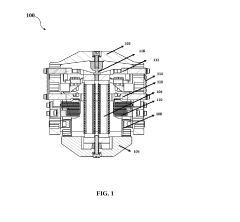
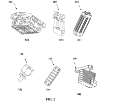
Mechanically enhanced high precision linear actuation device for space borne payloads
PatentActiveIN202441030336A
Innovation
- A mechanically enhanced high precision linear actuation device utilizing a stack of piezoelectric actuators, dumbbell flexures, multiplier flexures, flexure arms, sheet flexures, and back springs made of titanium alloy Ti6Al4V, which multiplies input linear motion through kinematic hinges and converts rotary motion to linear motion, allowing for tuning of output frequency and displacement without mechanical wear or backlash, and is designed to withstand space and launch vehicle environments.
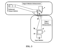
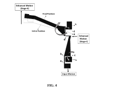
Differential compliant displacement reducer with output in same direction or reverse direction of input
PatentActiveUS11806870B2
Innovation
- A modular differential compliant displacement reducer is introduced, comprising a forward motion module and a reverse motion module with symmetrical structures, such as double-lever and half-bridge modules, connected through compliant hinges, which allows for differential superposition of displacement, enhancing the displacement reduction ratio and precision.
Applications of Piezoelectric Nanopositioning
Piezoelectric nanopositioning techniques have found widespread applications across various fields, revolutionizing precision control and measurement at the nanoscale. In the semiconductor industry, these techniques are crucial for lithography processes, enabling the precise positioning of wafers and masks to achieve high-resolution patterns. This level of accuracy is essential for manufacturing increasingly smaller and more complex integrated circuits.
In the field of microscopy, piezoelectric nanopositioning systems have greatly enhanced the capabilities of scanning probe microscopes, such as atomic force microscopes (AFM) and scanning tunneling microscopes (STM). These systems allow for precise control of the probe tip, enabling high-resolution imaging and manipulation of individual atoms and molecules. This has led to significant advancements in materials science, nanotechnology, and surface characterization.
Biomedical research has also benefited from piezoelectric nanopositioning techniques. In optical microscopy, these systems are used for focus control and sample positioning, enabling high-resolution imaging of biological specimens. Additionally, piezoelectric nanopositioners are employed in cell manipulation and microinjection techniques, allowing researchers to precisely control the placement of probes and deliver substances to specific cellular locations.
In the field of optics and photonics, piezoelectric nanopositioning is essential for aligning optical components with nanometer-level precision. This is particularly important in the development of advanced laser systems, optical communication devices, and quantum optics experiments. The ability to precisely control the position of mirrors, lenses, and other optical elements has led to improvements in beam steering, interferometry, and adaptive optics systems.
Precision manufacturing industries, such as aerospace and automotive, utilize piezoelectric nanopositioning for quality control and metrology applications. These techniques enable high-precision measurements of surface profiles, dimensions, and material properties, ensuring strict adherence to manufacturing tolerances. In addition, piezoelectric nanopositioners are used in advanced machining processes, such as ultra-precision cutting and grinding, to achieve nanometer-level accuracy in component fabrication.
The field of data storage has also benefited from piezoelectric nanopositioning techniques. In hard disk drives, these systems are used for precise head positioning, enabling higher data storage densities and faster read/write speeds. Similarly, in optical data storage systems, piezoelectric nanopositioners are employed for precise focusing and tracking of laser beams, improving the reliability and capacity of optical discs.
As the demand for miniaturization and precision continues to grow across various industries, the applications of piezoelectric nanopositioning techniques are expected to expand further. Emerging fields such as nanorobotics, quantum computing, and advanced sensing technologies are likely to drive new innovations and applications in this area, highlighting the continued importance of piezoelectric sensors in driving nanopositioning techniques.
Precision and Accuracy Considerations
Precision and accuracy are paramount considerations in nanopositioning techniques driven by piezoelectric sensors. The ability to achieve and maintain precise positioning at the nanoscale level is crucial for various applications, including microscopy, semiconductor manufacturing, and scientific research. Piezoelectric sensors offer unique advantages in this domain due to their high sensitivity and rapid response times.
One of the primary challenges in nanopositioning is minimizing positioning errors. These errors can arise from various sources, including thermal drift, mechanical vibrations, and electrical noise. Piezoelectric sensors must be carefully calibrated and integrated into feedback control systems to compensate for these errors and maintain accurate positioning. Advanced control algorithms, such as proportional-integral-derivative (PID) controllers or more sophisticated adaptive control methods, are often employed to optimize the sensor's performance.
The resolution of piezoelectric sensors is another critical factor in nanopositioning applications. The sensor's ability to detect minute changes in position directly impacts the overall system's precision. Modern piezoelectric sensors can achieve sub-nanometer resolution, enabling extremely fine control over positioning. However, this high resolution must be balanced with the sensor's dynamic range to ensure it can operate effectively across the required positioning range.
Environmental factors play a significant role in the precision and accuracy of nanopositioning systems. Temperature fluctuations, in particular, can cause thermal expansion or contraction of materials, leading to positioning errors. To mitigate these effects, temperature compensation techniques are often implemented, either through hardware design or software algorithms. Additionally, vibration isolation systems are frequently employed to minimize the impact of external mechanical disturbances on the positioning accuracy.
The linearity of piezoelectric sensors is another important consideration. While piezoelectric materials exhibit excellent sensitivity, they can also display nonlinear behavior, especially when operated over large ranges or at high frequencies. This nonlinearity can introduce errors in position measurements and control. Techniques such as charge amplification and feedback linearization are used to address these issues and improve the overall system performance.
Long-term stability and repeatability are essential for many nanopositioning applications. Piezoelectric sensors may experience drift over time due to material aging or environmental factors. Regular calibration and the use of reference standards are necessary to maintain accuracy over extended periods. Additionally, hysteresis effects in piezoelectric materials can impact repeatability, requiring compensation techniques to ensure consistent positioning performance.
In conclusion, achieving high precision and accuracy in nanopositioning techniques driven by piezoelectric sensors requires a multifaceted approach. It involves careful sensor selection, advanced control strategies, environmental management, and ongoing calibration and maintenance. By addressing these considerations, researchers and engineers can harness the full potential of piezoelectric sensors to drive nanopositioning techniques with unprecedented precision and reliability.
Unlock deeper insights with Patsnap Eureka Quick Research — get a full tech report to explore trends and direct your research. Try now!
Generate Your Research Report Instantly with AI Agent
Supercharge your innovation with Patsnap Eureka AI Agent Platform!