How to Design Frequency-Locked Loop for Compact Wearable Devices
MAR 18, 20269 MIN READ
Generate Your Research Report Instantly with AI Agent
PatSnap Eureka helps you evaluate technical feasibility & market potential.
FLL Design Challenges and Goals for Wearable Devices
The design of frequency-locked loops for compact wearable devices presents a unique set of engineering challenges that stem from the fundamental constraints of miniaturized electronics. The primary challenge lies in achieving stable frequency synchronization within severely limited physical dimensions, where traditional FLL architectures must be reimagined to accommodate space constraints while maintaining performance standards. Power consumption emerges as another critical challenge, as wearable devices operate on limited battery capacity and require extended operational periods without frequent charging cycles.
Thermal management represents a significant design hurdle in compact wearable implementations. The close proximity of components in miniaturized designs creates heat concentration issues that can adversely affect FLL stability and accuracy. Additionally, the dynamic operating environment of wearable devices introduces mechanical stress and vibration factors that can impact frequency stability, requiring robust design approaches to maintain consistent performance across various user activities and environmental conditions.
Signal integrity becomes increasingly challenging as component density increases and interconnect lengths are minimized. The reduced spacing between circuit elements can lead to increased electromagnetic interference and crosstalk, potentially degrading FLL performance. Manufacturing tolerances also become more critical in compact designs, where small variations in component values or placement can significantly impact overall system performance.
The primary goal for FLL design in wearable devices is to achieve optimal frequency tracking accuracy while minimizing power consumption and physical footprint. This requires innovative circuit topologies that can deliver comparable performance to larger implementations while operating within strict power budgets. The design must also prioritize integration capabilities, enabling seamless incorporation with other wearable device subsystems such as sensors, communication modules, and processing units.
Reliability and robustness constitute essential design goals, as wearable devices must function consistently across diverse environmental conditions including temperature variations, humidity changes, and physical movement. The FLL must maintain stable operation throughout the device's expected lifetime while withstanding the mechanical stresses associated with daily wear patterns.
Cost optimization represents another crucial goal, as wearable devices target consumer markets where price sensitivity is significant. This necessitates design approaches that minimize component count and complexity while leveraging standard manufacturing processes to achieve economies of scale.
Market Demand for Compact Wearable Electronics
The global wearable electronics market has experienced unprecedented growth driven by increasing consumer awareness of health monitoring, fitness tracking, and connected lifestyle preferences. Smartwatches, fitness trackers, hearables, and medical monitoring devices represent the primary segments demanding compact, power-efficient frequency-locked loop solutions for reliable wireless communication and sensor data processing.
Healthcare applications constitute a rapidly expanding segment where precise frequency control becomes critical for continuous monitoring devices. Wearable ECG monitors, glucose sensors, and blood pressure tracking devices require stable frequency references to ensure accurate data transmission to healthcare providers and mobile applications. The aging global population and rising chronic disease prevalence amplify demand for medical-grade wearable devices with extended battery life and miniaturized form factors.
Consumer fitness and wellness markets drive substantial demand for multi-functional wearables integrating GPS tracking, heart rate monitoring, and smartphone connectivity. These devices necessitate frequency-locked loops capable of managing multiple communication protocols simultaneously while maintaining compact dimensions and low power consumption. The trend toward always-on connectivity and real-time data synchronization intensifies requirements for robust frequency stability across varying environmental conditions.
Enterprise and industrial applications present emerging opportunities for specialized wearable devices in manufacturing, logistics, and safety monitoring sectors. Worker safety devices, asset tracking wearables, and industrial IoT sensors require frequency-locked loops optimized for harsh operating environments while maintaining reliable communication links with enterprise networks.
The convergence of artificial intelligence, edge computing, and wearable technology creates new market segments demanding advanced frequency control solutions. Smart clothing, augmented reality glasses, and biometric authentication devices represent next-generation applications requiring sophisticated frequency management capabilities within increasingly constrained physical spaces.
Market growth drivers include technological miniaturization advances, declining component costs, improved battery technologies, and expanding wireless communication standards. Consumer expectations for seamless connectivity, extended battery life, and enhanced functionality continue pushing manufacturers toward more efficient frequency-locked loop implementations that can deliver superior performance within compact wearable form factors.
Current State and Limitations of FLL in Wearables
Frequency-locked loops in contemporary wearable devices predominantly rely on traditional phase-locked loop architectures adapted for lower power consumption. Current implementations typically utilize CMOS-based voltage-controlled oscillators operating in the sub-GHz to low-GHz frequency ranges, with power consumption ranging from 0.5mW to 5mW depending on the application requirements. These systems generally achieve frequency accuracy within ±20ppm to ±50ppm under normal operating conditions.
The integration density constraints of wearable form factors have led to significant compromises in FLL performance characteristics. Most existing solutions occupy silicon areas between 0.1mm² to 0.5mm², which limits the implementation of sophisticated loop filtering and noise reduction techniques. The reduced component count directly impacts phase noise performance, typically resulting in phase noise floors of -90dBc/Hz to -110dBc/Hz at 1MHz offset frequencies.
Power management represents the most critical limitation in current wearable FLL implementations. Battery capacity constraints necessitate ultra-low power operation, yet maintaining frequency stability requires continuous oscillator operation and periodic calibration cycles. This fundamental trade-off results in either compromised frequency accuracy or reduced battery life, with most commercial solutions prioritizing power efficiency over precision timing performance.
Temperature stability poses another significant challenge for compact wearable FLL designs. The limited thermal mass and direct skin contact create rapid temperature variations that exceed the compensation capabilities of standard temperature-compensated crystal oscillators. Current solutions exhibit frequency drift coefficients of ±10ppm to ±25ppm across the typical operating temperature range of 15°C to 45°C, which proves insufficient for precision timing applications.
Manufacturing variability and component aging effects are amplified in miniaturized FLL implementations due to the reduced averaging effects of smaller component geometries. Process variations can result in initial frequency errors exceeding ±100ppm before calibration, requiring extensive factory trimming procedures that increase production costs and complexity.
The electromagnetic interference susceptibility of compact FLL circuits presents additional operational challenges in wearable environments. The proximity to switching power supplies, wireless communication modules, and external interference sources can cause frequency pulling effects and increased jitter performance, particularly in designs lacking adequate shielding or filtering capabilities.
Existing FLL Solutions for Compact Device Integration
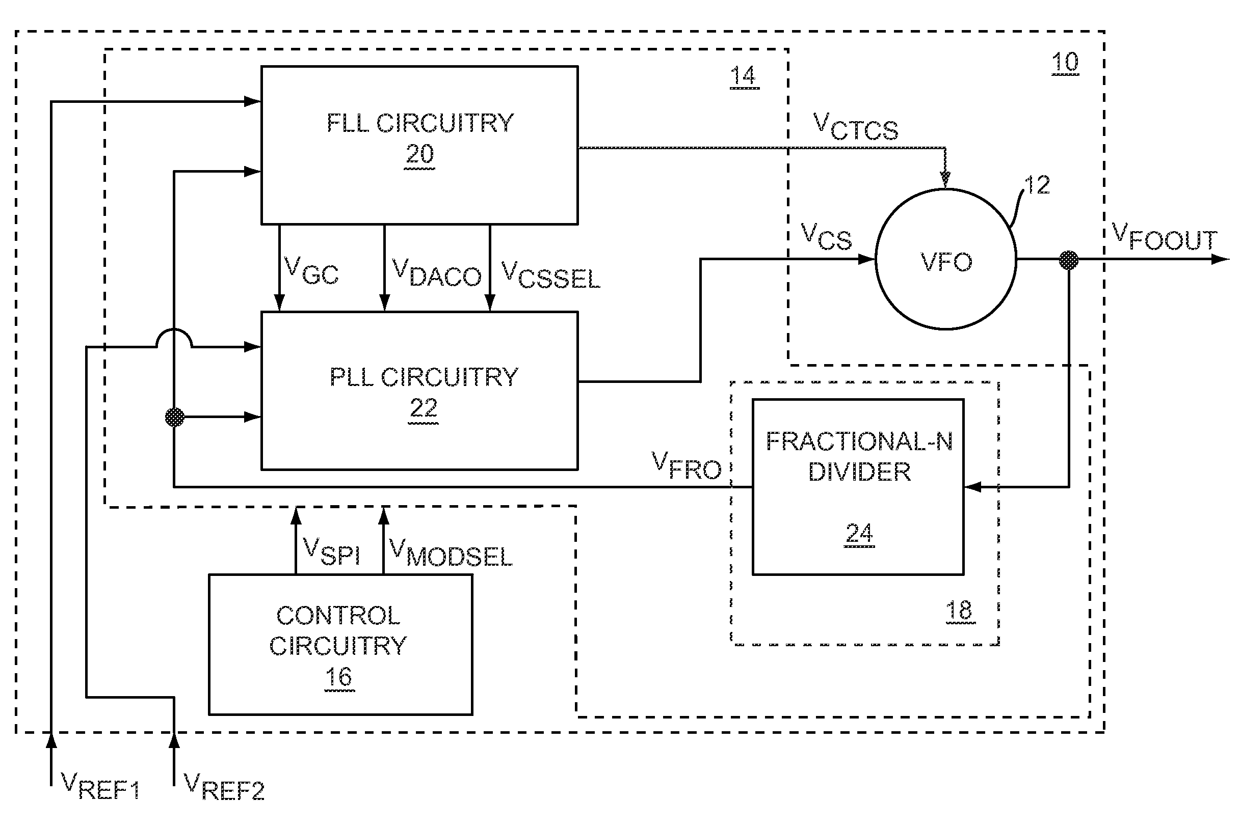
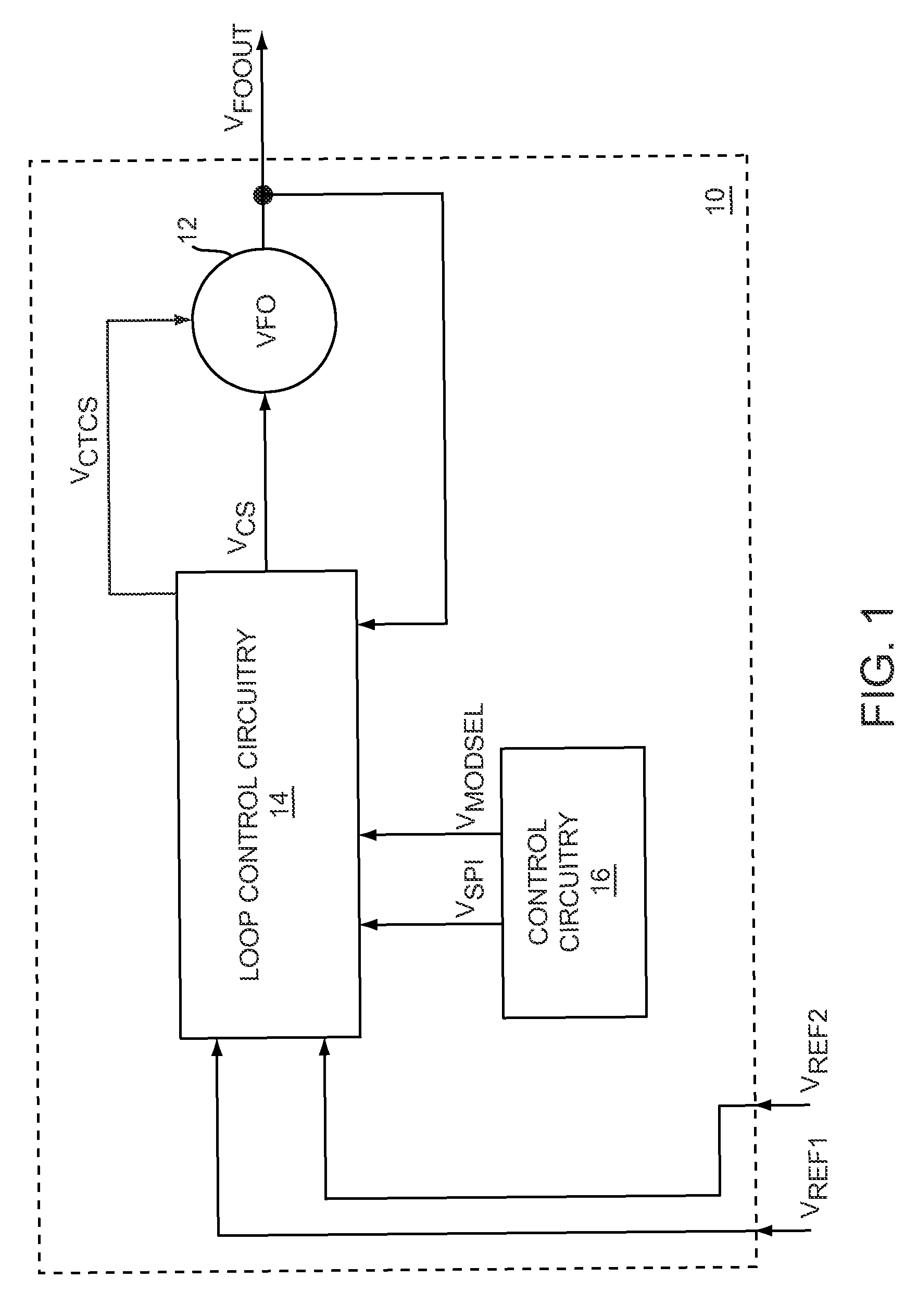
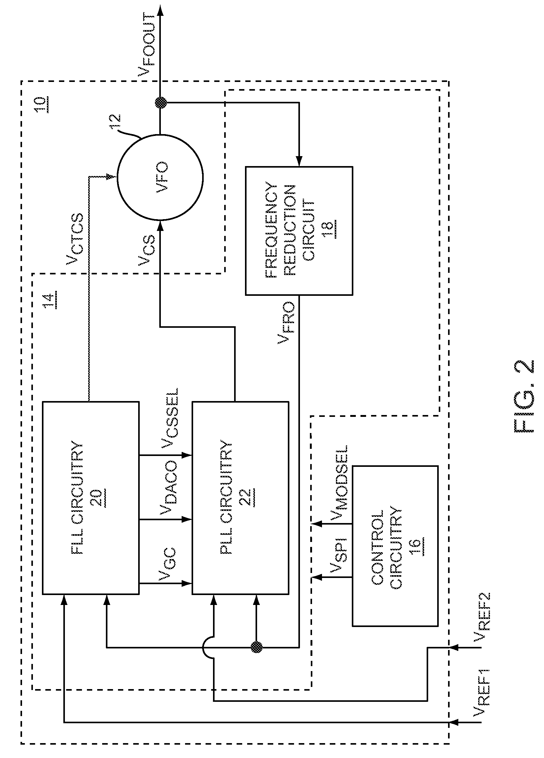
01 Frequency-locked loop circuit architecture and design
Frequency-locked loop circuits are designed with specific architectures to achieve frequency locking between input and output signals. These circuits typically include components such as frequency detectors, phase comparators, and voltage-controlled oscillators arranged in feedback configurations. The architecture enables the system to detect frequency differences and adjust the output frequency to match or maintain a specific relationship with the input frequency. Various circuit topologies and design approaches can be employed to optimize performance characteristics such as lock range, acquisition time, and stability.- Frequency-locked loop circuit architecture and design: Frequency-locked loop (FLL) circuits provide an alternative to phase-locked loops (PLLs) for frequency synthesis and synchronization applications. These circuits lock to the frequency of an input signal rather than its phase, offering advantages in certain applications such as reduced sensitivity to phase noise and faster lock times. The basic architecture typically includes a frequency detector, loop filter, and voltage-controlled oscillator (VCO). Various circuit topologies and design methodologies have been developed to optimize performance parameters such as lock range, lock time, and frequency accuracy.
- Frequency detection and comparison techniques: The frequency detector is a critical component in frequency-locked loop systems, responsible for comparing the input frequency with the output frequency and generating an error signal. Various frequency detection methods have been developed, including digital frequency discriminators, quadrature detection techniques, and edge-based frequency comparison circuits. These techniques enable accurate frequency measurement and comparison across wide frequency ranges while maintaining low power consumption and high linearity. Advanced detection methods incorporate digital signal processing to improve noise immunity and detection accuracy.
- Loop filter design and stability control: Loop filter design is essential for ensuring stability and optimal transient response in frequency-locked loop systems. The loop filter processes the error signal from the frequency detector to control the VCO and maintain frequency lock. Various filter topologies including active and passive designs have been implemented to achieve desired bandwidth, damping characteristics, and noise filtering. Adaptive loop filter techniques dynamically adjust filter parameters based on operating conditions to optimize performance across different frequency ranges and environmental conditions.
- Digital frequency-locked loop implementation: Digital implementations of frequency-locked loops offer advantages including programmability, reduced component count, and improved integration with digital systems. These implementations utilize digital frequency detectors, digital loop filters, and digitally-controlled oscillators. All-digital frequency-locked loop architectures employ time-to-digital converters and digital control logic to achieve frequency locking without analog components. Digital techniques enable features such as automatic frequency calibration, adaptive bandwidth control, and built-in self-test capabilities.
- Applications in communication and clock generation systems: Frequency-locked loops are widely used in communication systems, clock generation circuits, and frequency synthesis applications. In wireless communication systems, they enable carrier frequency recovery and clock synchronization. For clock generation, they provide stable reference frequencies for digital systems and data converters. Frequency-locked loops are particularly useful in applications requiring fast frequency acquisition, such as frequency hopping systems and burst-mode communications. They also find applications in clock and data recovery circuits, where they extract timing information from data streams.
02 Frequency detection and comparison methods
Frequency-locked loops employ various methods for detecting and comparing frequencies to generate control signals. These methods include digital frequency detection techniques, analog frequency comparison circuits, and hybrid approaches. The frequency detector measures the difference between reference and feedback frequencies and produces an error signal proportional to the frequency deviation. Advanced detection methods may incorporate edge detection, pulse counting, or digital signal processing techniques to improve accuracy and reduce noise sensitivity.Expand Specific Solutions03 Voltage-controlled oscillator integration and control
The voltage-controlled oscillator is a critical component in frequency-locked loop systems, converting control voltage into output frequency. Integration techniques focus on optimizing the oscillator's tuning range, linearity, and stability. Control mechanisms are designed to adjust the oscillator frequency based on error signals from the frequency detector. Various oscillator types can be utilized, including ring oscillators, LC oscillators, and digitally-controlled oscillators, each offering different performance trade-offs in terms of frequency range, power consumption, and phase noise.Expand Specific Solutions04 Digital frequency-locked loop implementation
Digital implementations of frequency-locked loops utilize digital signal processing techniques and digital control circuits to achieve frequency locking. These systems may employ digital frequency detectors, digital filters, and numerically-controlled oscillators. Digital approaches offer advantages such as programmability, reduced sensitivity to component variations, and easier integration with digital systems. Implementation methods include fully digital architectures as well as hybrid systems combining digital control with analog oscillators.Expand Specific Solutions05 Applications in communication and clock generation systems
Frequency-locked loops find extensive applications in communication systems and clock generation circuits. In communication applications, they are used for frequency synthesis, carrier recovery, and clock data recovery. For clock generation, frequency-locked loops provide stable reference frequencies and enable frequency multiplication or division. These systems are employed in wireless transceivers, data communication interfaces, and timing circuits where precise frequency control and synchronization are required. Implementation considerations include lock acquisition speed, jitter performance, and power efficiency.Expand Specific Solutions
Key Players in Wearable FLL and RF Components
The frequency-locked loop design for compact wearable devices represents a rapidly evolving market segment driven by the proliferation of IoT and health monitoring applications. The industry is in a growth phase, with the global wearable technology market expanding significantly as consumer demand for fitness trackers, smartwatches, and medical devices increases. Major technology companies like Huawei Technologies, Qualcomm, Samsung Electro-Mechanics, and Sony Group Corp. are leading innovation in this space, while semiconductor specialists including Texas Instruments, Infineon Technologies, and STMicroelectronics provide critical component solutions. The technology maturity varies across applications, with established players like Philips and Siemens contributing medical-grade solutions, while emerging companies focus on consumer applications. Research institutions such as South China University of Technology and Zhejiang University are advancing fundamental research, indicating strong academic-industry collaboration in developing next-generation frequency control solutions for miniaturized wearable platforms.
QUALCOMM, Inc.
Technical Solution: QUALCOMM has developed advanced frequency-locked loop (FLL) architectures specifically optimized for compact wearable devices. Their approach utilizes ultra-low power digital FLL designs that can operate with supply voltages as low as 0.6V while maintaining frequency accuracy within ±50ppm across temperature variations. The company implements adaptive bandwidth control mechanisms that dynamically adjust loop parameters based on environmental conditions and power constraints. Their FLL solutions integrate seamlessly with their Snapdragon Wear platforms, featuring sub-1mW power consumption and fast lock times under 100μs, making them ideal for smartwatches and fitness trackers where battery life is critical.
Strengths: Industry-leading low power consumption, excellent integration with existing SoC platforms, proven track record in mobile devices. Weaknesses: Higher licensing costs, potential vendor lock-in with proprietary solutions.
MediaTek Singapore Pte Ltd.
Technical Solution: MediaTek has integrated sophisticated FLL designs into their wearable SoC platforms, focusing on multi-standard compatibility and energy efficiency. Their frequency-locked loop architecture supports simultaneous operation of multiple wireless protocols (WiFi, Bluetooth, cellular) while maintaining tight frequency synchronization. The design incorporates advanced digital signal processing algorithms for rapid frequency acquisition and tracking, with lock times typically under 50μs. MediaTek's FLL implementation features dynamic power scaling that adjusts operating parameters based on real-time performance requirements, enabling up to 40% power savings during low-activity periods. The solution includes integrated clock generation for system-wide timing distribution in compact wearable devices.
Strengths: Strong integration with wireless connectivity solutions, competitive pricing, good power management features. Weaknesses: Less established in premium wearable market, limited customization options for specialized applications.
Core Innovations in Low-Power FLL Design
Frequency locked loop with fast reaction time
PatentInactiveUS20190165797A1
Innovation
- A frequency locked loop design featuring a digitally controlled oscillator, frequency counter and sequencer circuit, and controller with a variable frequency clock signal, utilizing a resynchronization circuit and trigger signal to synchronize phases and reduce iteration time by allowing early initiation of counting phases post-computation.


Frequency-locked loop calibration of a phase-locked loop gain
PatentInactiveUS7898343B1
Innovation
- A calibrated phase-locked loop (PLL) system with a calibration mode for measuring tuning gain and a PLL mode for normal operation, using frequency-locked loop (FLL) circuit elements for coarse tuning and PLL for high frequency accuracy, reducing phase lock times by regulating loop gain and pre-charging the PLL loop filter.

Power Consumption Optimization Strategies
Power consumption optimization represents the most critical design challenge for frequency-locked loops in wearable devices, where battery life directly impacts user experience and device adoption. The inherent trade-off between loop performance and energy efficiency requires sophisticated strategies that balance settling time, phase noise, and power dissipation within the constraints of miniaturized form factors.
Dynamic power scaling emerges as a fundamental optimization approach, enabling FLL circuits to adapt their power consumption based on operational requirements. This technique involves implementing multiple power modes where the loop can operate at reduced current levels during steady-state conditions and increase power only during acquisition or tracking phases. Advanced implementations utilize predictive algorithms that anticipate frequency changes, allowing preemptive power adjustments.
Circuit-level optimization focuses on reducing static and dynamic power consumption through architectural innovations. Low-power voltage-controlled oscillators utilizing subthreshold operation can achieve significant power reductions while maintaining acceptable phase noise performance. Additionally, implementing duty-cycled operation modes allows the FLL to periodically enter sleep states, particularly effective in applications with predictable reference patterns or when frequency stability requirements permit intermittent operation.
Supply voltage optimization plays a crucial role in power reduction strategies. Near-threshold voltage operation, combined with adaptive body biasing techniques, can reduce power consumption by orders of magnitude. However, this approach requires careful consideration of process variations and temperature effects, necessitating robust design margins and compensation circuits that maintain loop stability across operating conditions.
Advanced power management incorporates intelligent control algorithms that monitor loop performance metrics and dynamically adjust circuit parameters. These systems can optimize bias currents, bandwidth settings, and update rates based on real-time assessment of frequency drift rates and environmental conditions. Machine learning approaches show promise in predicting optimal power allocation patterns based on usage history and contextual information from other device sensors.
Electromagnetic Interference Mitigation Approaches
Electromagnetic interference (EMI) poses significant challenges for frequency-locked loops (FLLs) in compact wearable devices, where space constraints and proximity to various electronic components create complex interference scenarios. The miniaturized form factor of wearables necessitates sophisticated EMI mitigation strategies that balance performance, power consumption, and physical footprint limitations.
Shielding techniques represent the primary defense mechanism against external EMI sources. Advanced micro-shielding approaches utilize thin metallic films and conductive polymers to create localized electromagnetic barriers around critical FLL components. These materials, typically copper or silver-based coatings with thicknesses ranging from 10-50 micrometers, provide effective attenuation while maintaining the compact profile essential for wearable applications.
Grounding strategies play a crucial role in EMI suppression within FLL circuits. Multi-layer PCB designs incorporate dedicated ground planes and strategic via placement to minimize ground loops and reduce common-mode interference. Star grounding configurations, where all circuit sections connect to a single ground point, prove particularly effective in preventing interference coupling between different functional blocks of the FLL system.
Filtering methodologies encompass both passive and active approaches to eliminate unwanted frequency components. Low-pass filters positioned at critical input and output stages of the FLL effectively attenuate high-frequency noise while preserving signal integrity. Ferrite beads and common-mode chokes provide additional suppression for conducted EMI, particularly effective against switching noise from power management circuits commonly found in wearable devices.
Circuit topology optimization involves strategic component placement and routing techniques to minimize EMI susceptibility. Differential signaling architectures inherently reject common-mode interference, making them ideal for FLL implementations in noisy wearable environments. Additionally, careful consideration of trace impedance matching and minimization of loop areas reduces both radiated emissions and susceptibility to external interference sources.
Power supply decoupling represents another critical mitigation approach, utilizing strategically placed capacitors to suppress power rail noise that can degrade FLL performance. Multiple capacitor values, ranging from picofarads to microfarads, address different frequency ranges of potential interference, ensuring clean power delivery to sensitive analog components within the frequency-locked loop architecture.
Unlock deeper insights with PatSnap Eureka Quick Research — get a full tech report to explore trends and direct your research. Try now!
Generate Your Research Report Instantly with AI Agent
Supercharge your innovation with PatSnap Eureka AI Agent Platform!