Implementation Insights for Computational Lithography in Aerospace
APR 24, 20269 MIN READ
Generate Your Research Report Instantly with AI Agent
PatSnap Eureka helps you evaluate technical feasibility & market potential.
Computational Lithography Background and Aerospace Goals
Computational lithography represents a revolutionary convergence of advanced mathematical modeling, optical physics, and semiconductor manufacturing processes that has fundamentally transformed the precision manufacturing landscape over the past three decades. This technology emerged from the critical need to overcome the physical limitations of traditional photolithography as feature sizes approached and surpassed the wavelength of light used in the patterning process.
The foundational principles of computational lithography rest upon sophisticated algorithms that predict and compensate for optical proximity effects, diffraction phenomena, and process variations inherent in nanoscale manufacturing. Through the integration of inverse lithography technology, optical proximity correction, and source mask optimization, this field has enabled the continuation of Moore's Law well beyond what conventional lithography could achieve.
The aerospace industry presents unique and demanding requirements that distinguish it from traditional semiconductor applications. Unlike consumer electronics where cost optimization and high-volume production dominate design considerations, aerospace applications prioritize extreme reliability, radiation hardness, and performance consistency across wide temperature ranges and harsh environmental conditions.
Current aerospace manufacturing faces unprecedented challenges in producing next-generation components for satellite systems, avionics, and propulsion control units. The industry requires manufacturing capabilities that can achieve sub-10-nanometer precision while maintaining the stringent quality standards necessary for mission-critical applications where failure is not an option.
The primary technological objectives for implementing computational lithography in aerospace manufacturing encompass several critical areas. First, achieving enhanced pattern fidelity for complex three-dimensional structures used in advanced sensor arrays and communication systems. Second, developing robust process control methodologies that can maintain consistent performance across extended production runs while accommodating the specialized materials commonly used in aerospace applications.
Furthermore, the integration of computational lithography aims to enable the production of novel device architectures specifically designed for space environments, including radiation-hardened integrated circuits and high-frequency components for next-generation satellite communication systems. These objectives require advancing beyond current computational models to incorporate aerospace-specific material properties and environmental stress factors.
The ultimate goal involves establishing a comprehensive manufacturing ecosystem that leverages computational lithography's predictive capabilities to reduce development cycles, minimize prototype iterations, and ensure first-pass manufacturing success for aerospace components where traditional trial-and-error approaches are prohibitively expensive and time-consuming.
Market Demand for Advanced Aerospace Manufacturing
The aerospace manufacturing sector is experiencing unprecedented demand for precision components that require nanometer-level accuracy, driving significant market opportunities for computational lithography technologies. Modern aircraft engines, satellite systems, and spacecraft rely heavily on microelectromechanical systems (MEMS), advanced sensors, and miniaturized electronic components that demand manufacturing tolerances previously achievable only in semiconductor fabrication facilities.
Commercial aerospace markets are particularly driving demand for lightweight, high-performance components that integrate multiple functionalities into compact form factors. Next-generation aircraft engines require sophisticated sensor arrays, fuel injection systems, and control mechanisms that benefit from lithographic manufacturing precision. The push toward more electric aircraft architectures has intensified requirements for advanced power electronics and control systems manufactured with computational lithography techniques.
Defense and space applications represent another substantial market driver, where mission-critical components must meet extreme reliability standards while maintaining minimal size and weight constraints. Satellite constellations, deep space missions, and military aircraft systems increasingly depend on components manufactured using advanced lithographic processes to achieve required performance specifications within strict dimensional and weight limitations.
The market demand extends beyond traditional electronic components to include specialized aerospace applications such as micro-propulsion systems, advanced thermal management solutions, and integrated optical systems for navigation and communication. These applications require manufacturing capabilities that can produce complex three-dimensional structures with precise material properties and surface characteristics achievable through computational lithography approaches.
Supply chain considerations are also driving market demand, as aerospace manufacturers seek to reduce dependency on traditional semiconductor foundries by developing in-house or dedicated aerospace-focused lithographic manufacturing capabilities. This trend reflects both security concerns and the need for specialized processes optimized for aerospace-specific materials and performance requirements rather than conventional silicon-based electronics.
The growing emphasis on sustainable aviation technologies and electric propulsion systems further amplifies demand for advanced manufacturing techniques. These emerging technologies require novel component designs and material combinations that push the boundaries of conventional manufacturing methods, creating substantial market opportunities for computational lithography implementation in aerospace manufacturing environments.
Current State of Computational Lithography in Aerospace
Computational lithography in aerospace applications currently represents a specialized intersection of advanced semiconductor manufacturing techniques and the stringent requirements of space-grade electronics. The technology has evolved from traditional photolithography methods to incorporate sophisticated computational algorithms that optimize pattern fidelity, process margins, and yield for aerospace-specific integrated circuits and microelectromechanical systems.
The present landscape is characterized by the adaptation of established computational lithography techniques, including optical proximity correction, phase-shift masking, and source mask optimization, to meet the unique demands of aerospace environments. These adaptations address challenges such as radiation hardening, extreme temperature variations, and long-term reliability requirements that exceed commercial semiconductor specifications.
Current implementations primarily focus on enhancing the manufacturability of radiation-hardened integrated circuits and specialized sensors used in satellite systems, spacecraft control units, and navigation equipment. The technology enables the production of smaller feature sizes while maintaining the robustness necessary for space applications, where component failure can have catastrophic consequences.
Leading aerospace manufacturers and their semiconductor partners have developed proprietary computational lithography workflows that incorporate space-environment modeling into the design and manufacturing process. These workflows utilize advanced simulation tools to predict and compensate for potential failure modes specific to space applications, including single-event upsets and total ionizing dose effects.
The integration of machine learning algorithms into computational lithography processes has emerged as a significant advancement, enabling real-time optimization of manufacturing parameters based on historical performance data from deployed aerospace systems. This approach has demonstrated improvements in yield rates and long-term reliability metrics compared to conventional manufacturing approaches.
Despite these advances, current implementations face limitations in terms of computational complexity and processing time, particularly when dealing with the extensive design rule checks required for aerospace applications. The need for comprehensive verification and validation processes, mandated by aerospace quality standards, adds additional layers of complexity to the computational lithography workflow.
The technology's current state reflects a balance between leveraging cutting-edge semiconductor manufacturing capabilities and maintaining the conservative, reliability-focused approach characteristic of aerospace engineering practices.
Existing Computational Lithography Solutions
01 Optical proximity correction (OPC) techniques
Computational lithography methods employ optical proximity correction to compensate for diffraction effects and process variations in photolithography. These techniques use mathematical models and algorithms to modify mask patterns, predicting how light will interact with photoresist and adjusting designs accordingly. Advanced OPC methods incorporate machine learning and iterative optimization to improve pattern fidelity and reduce critical dimension variations across the wafer.- Optical proximity correction (OPC) techniques: Computational lithography methods employ optical proximity correction to compensate for diffraction effects and process variations in photolithography. These techniques use algorithms to modify mask patterns by adding sub-resolution assist features, adjusting edge positions, and optimizing feature shapes to ensure that the printed patterns on wafers match the intended design. Advanced OPC methods incorporate machine learning and model-based approaches to predict and correct pattern distortions before mask fabrication.
- Source mask optimization (SMO): Source mask optimization is a computational technique that simultaneously optimizes both the illumination source and mask patterns to achieve better lithographic performance. This approach considers the interaction between source shapes and mask features to maximize process windows, improve pattern fidelity, and enhance depth of focus. The optimization process typically involves iterative algorithms that balance multiple objectives including contrast, image quality, and manufacturing constraints.
- Inverse lithography technology (ILT): Inverse lithography technology represents an advanced computational approach that works backward from the desired wafer pattern to determine optimal mask shapes. Unlike traditional rule-based methods, ILT uses pixel-based optimization and mathematical algorithms to generate mask patterns that may appear counterintuitive but produce superior results on wafer. This technology enables the creation of complex curvilinear mask features that maximize lithographic performance for advanced technology nodes.
- Machine learning and AI-based lithography modeling: Modern computational lithography incorporates artificial intelligence and machine learning algorithms to improve prediction accuracy and reduce computation time. These methods use neural networks, deep learning, and pattern recognition to model complex lithographic processes, predict hotspots, and optimize correction strategies. AI-based approaches can learn from historical manufacturing data to continuously improve model accuracy and adapt to process variations.
- Multi-patterning decomposition and verification: Computational methods for multi-patterning lithography involve decomposing complex patterns into multiple mask layers that can be printed separately and combined on the wafer. These techniques address the limitations of single-exposure lithography at advanced nodes by using algorithms to assign features to different masks while minimizing conflicts and optimizing overlay requirements. Verification tools ensure that the decomposed patterns will produce the intended results while meeting manufacturing constraints.
02 Source mask optimization (SMO)
Source mask optimization is a computational approach that simultaneously optimizes both the illumination source and mask patterns to achieve better imaging performance. This technique uses inverse lithography principles and optimization algorithms to determine optimal source shapes and mask configurations. The method enables enhanced resolution, improved process windows, and better pattern transfer for advanced semiconductor manufacturing nodes.Expand Specific Solutions03 Machine learning and AI-based lithography modeling
Artificial intelligence and machine learning techniques are applied to lithography simulation and optimization processes. These methods use neural networks, deep learning models, and data-driven approaches to predict lithography outcomes, accelerate computational processes, and improve accuracy. The technology enables faster mask optimization, defect prediction, and process control through pattern recognition and predictive modeling.Expand Specific Solutions04 Inverse lithography technology (ILT)
Inverse lithography technology uses computational methods to work backwards from desired wafer patterns to determine optimal mask shapes. This approach employs mathematical optimization, pixel-based mask synthesis, and advanced algorithms to create non-intuitive mask patterns that produce superior on-wafer results. The technique provides enhanced resolution capabilities and improved process margins for complex pattern geometries.Expand Specific Solutions05 Computational process modeling and simulation
Comprehensive computational models simulate the entire lithography process including optical imaging, photoresist chemistry, and pattern development. These simulation tools incorporate physical models of light propagation, chemical reactions, and material properties to predict final pattern outcomes. Advanced simulation frameworks enable virtual process optimization, defect analysis, and yield prediction before actual wafer fabrication.Expand Specific Solutions
Key Players in Aerospace Computational Lithography
The computational lithography market for aerospace applications is experiencing rapid growth driven by increasing demand for advanced semiconductor components in aerospace systems. The industry is in a mature development stage with established market leaders like ASML Netherlands BV and Carl Zeiss SMT GmbH dominating lithography equipment manufacturing. Technology maturity varies significantly across players - while ASML and Synopsys represent cutting-edge EUV and computational lithography solutions, companies like Boeing and Airbus Defence & Space focus on aerospace integration. Semiconductor manufacturers including GLOBALFOUNDRIES, SMIC, and Applied Materials provide foundational manufacturing capabilities, while emerging players like D2S and Chinese companies such as ChangXin Memory Technologies are developing specialized solutions. The convergence of established aerospace giants with semiconductor technology leaders creates a competitive landscape where technological sophistication and aerospace-grade reliability requirements drive innovation and market positioning.
ASML Netherlands BV
Technical Solution: ASML leads computational lithography with advanced EUV systems featuring sophisticated optical proximity correction (OPC) and source mask optimization (SMO) algorithms. Their computational lithography solutions integrate machine learning-based process modeling with real-time aberration correction, enabling sub-7nm node manufacturing. The company's Brion acquisition strengthened their computational capabilities, providing comprehensive mask synthesis and process optimization tools that reduce manufacturing variability by up to 30% while improving yield rates for critical aerospace semiconductor components requiring extreme reliability and precision.
Strengths: Industry-leading EUV technology, comprehensive computational suite, strong R&D investment. Weaknesses: High equipment costs, complex implementation requirements, limited supplier diversity for aerospace applications.
Synopsys, Inc.
Technical Solution: Synopsys provides comprehensive computational lithography solutions through their Proteus platform, featuring advanced OPC, inverse lithography technology (ILT), and curvilinear mask optimization. Their aerospace-focused implementations include radiation-hardened design flows and specialized process models for high-reliability applications. The platform integrates machine learning algorithms for hotspot detection and correction, reducing design rule violations by 40-60%. Their computational engines support multi-patterning techniques essential for advanced node aerospace processors, with specialized thermal and stress modeling capabilities for space-grade semiconductor manufacturing.
Strengths: Comprehensive EDA ecosystem, strong machine learning integration, aerospace-specific design flows. Weaknesses: Software complexity requires extensive training, high licensing costs, dependency on foundry process data.
Core Innovations in Aerospace Lithography Patents
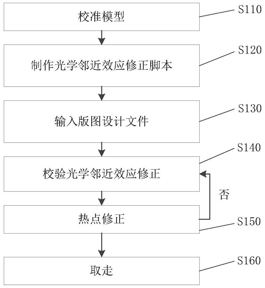
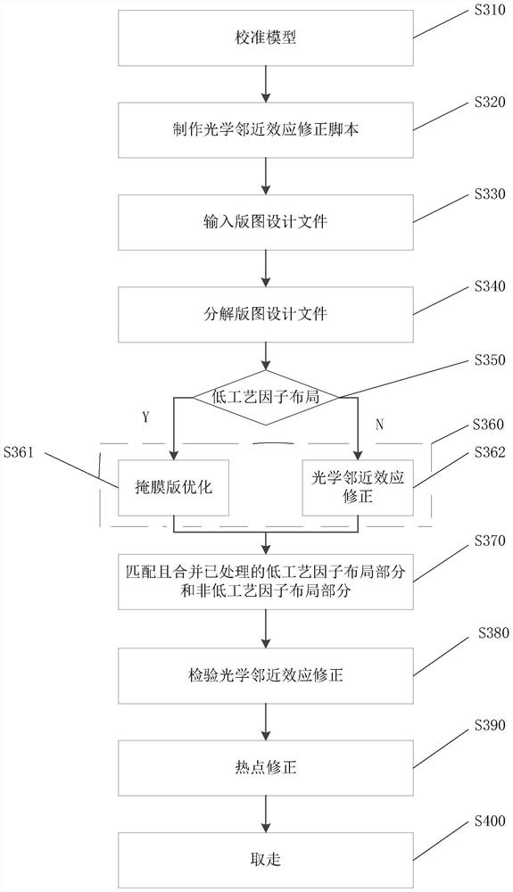
Computational lithography method and system for optical proximity correction
PatentActiveCN109932864B
Innovation
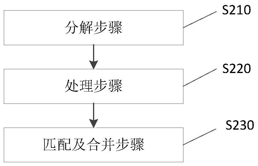
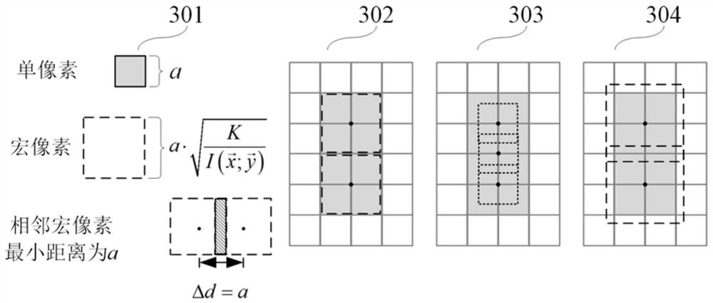
- By decomposing the layout design file into a first layout part with a process factor lower than the preset threshold and a second layout part with a process factor higher than the preset threshold, and processing and merging the two parts respectively, iteration steps are reduced and processing efficiency is improved.

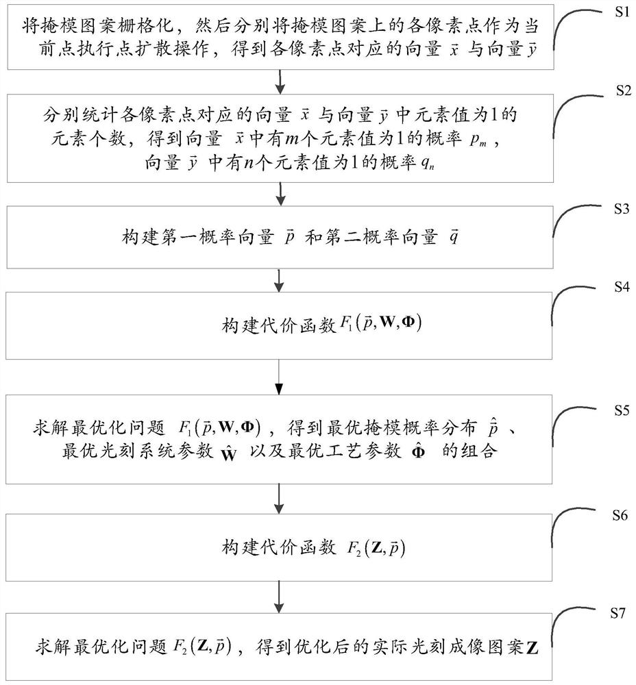
A computational photolithography method
PatentActiveCN112083631B
Innovation
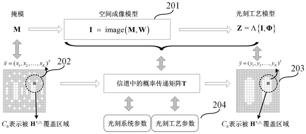
- Informatics computational lithography methods are used to establish a channel model through point diffusion operations, probability distribution construction and mutual information calculations to solve for optimal mask distribution, lithography system parameters and process parameters. Abstract lithography imaging is a channel transmission process and is optimized. Mask pattern to improve imaging accuracy.

Aerospace Industry Standards and Compliance
The aerospace industry operates under stringent regulatory frameworks that directly impact the implementation of computational lithography technologies. Primary governing bodies include the Federal Aviation Administration (FAA), European Union Aviation Safety Agency (EASA), and International Civil Aviation Organization (ICAO), each establishing comprehensive standards for manufacturing processes and component reliability. These regulations mandate rigorous documentation, traceability, and quality assurance protocols that computational lithography systems must accommodate.
AS9100 certification represents the cornerstone quality management standard for aerospace manufacturing, building upon ISO 9001 with additional aerospace-specific requirements. Computational lithography implementations must demonstrate compliance with configuration management, risk assessment, and continuous improvement processes outlined in AS9100. The standard emphasizes statistical process control and measurement system analysis, requiring lithography systems to provide detailed process monitoring and data logging capabilities.
Material specifications under standards such as AMS (Aerospace Material Specifications) and ASTM International directly influence lithography process parameters. These specifications define precise material properties, surface finish requirements, and dimensional tolerances that computational algorithms must achieve. Compliance necessitates integration of real-time feedback systems and adaptive process control to maintain consistency across production batches.
Cybersecurity compliance has emerged as a critical consideration following NIST Cybersecurity Framework adoption across aerospace supply chains. Computational lithography systems handling sensitive design data must implement robust access controls, encryption protocols, and audit trails. The framework requires regular vulnerability assessments and incident response procedures, particularly relevant for cloud-based computational resources.
Environmental regulations including REACH (Registration, Evaluation, Authorization and Restriction of Chemicals) and RoHS (Restriction of Hazardous Substances) impact material selection and process chemistry in lithography applications. Compliance documentation must demonstrate adherence to substance restrictions while maintaining performance specifications required for aerospace applications.
Export control regulations such as ITAR (International Traffic in Arms Regulations) and EAR (Export Administration Regulations) significantly influence technology transfer and international collaboration in computational lithography development. These regulations require careful classification of algorithms, software tools, and technical data, potentially restricting access to certain computational methods or requiring special licensing for cross-border projects.
Manufacturing Quality Control in Aerospace Lithography
Manufacturing quality control in aerospace lithography represents a critical intersection of precision engineering and advanced manufacturing processes, where computational lithography serves as both an enabler and a quality assurance mechanism. The aerospace industry's stringent requirements for component reliability and performance necessitate unprecedented levels of manufacturing precision, particularly in the production of microelectronic systems, sensors, and specialized optical components used in avionics and spacecraft systems.
The implementation of computational lithography in aerospace manufacturing introduces sophisticated quality control paradigms that extend beyond traditional inspection methods. Real-time process monitoring systems integrate advanced algorithms to predict and compensate for manufacturing variations during the lithography process itself. These systems employ machine learning models trained on historical production data to identify potential defects before they manifest in the final product, significantly reducing waste and improving yield rates.
Statistical process control methodologies specifically adapted for computational lithography environments utilize multi-dimensional data analysis to track process stability across various parameters including exposure dose uniformity, overlay accuracy, and critical dimension control. Advanced metrology systems equipped with high-resolution imaging capabilities provide sub-nanometer measurement precision, enabling the detection of minute variations that could compromise component performance in aerospace applications.
Traceability systems integrated with computational lithography platforms maintain comprehensive records of all process parameters, material batches, and environmental conditions throughout the manufacturing cycle. This level of documentation proves essential for aerospace certification requirements and enables rapid root cause analysis when quality issues arise. The systems also facilitate predictive maintenance scheduling for lithography equipment, minimizing unplanned downtime and maintaining consistent production quality.
Automated defect classification algorithms analyze pattern fidelity and dimensional accuracy in real-time, categorizing defects by severity and potential impact on final component functionality. These systems integrate with upstream design verification processes and downstream assembly operations, creating a closed-loop quality management system that continuously optimizes manufacturing parameters based on performance feedback from deployed aerospace systems.
Unlock deeper insights with PatSnap Eureka Quick Research — get a full tech report to explore trends and direct your research. Try now!
Generate Your Research Report Instantly with AI Agent
Supercharge your innovation with PatSnap Eureka AI Agent Platform!