Integration of Piezoelectric Sensors in MEMS Devices
JUL 17, 20259 MIN READ
Generate Your Research Report Instantly with AI Agent
Patsnap Eureka helps you evaluate technical feasibility & market potential.
MEMS Piezo Integration Background and Objectives
The integration of piezoelectric sensors in MEMS (Micro-Electro-Mechanical Systems) devices represents a significant advancement in the field of microsensors and actuators. This technology combines the precision and sensitivity of piezoelectric materials with the miniaturization and scalability of MEMS fabrication techniques. The development of this integration has its roots in the early 1990s when researchers began exploring ways to incorporate piezoelectric thin films into silicon-based microstructures.
The evolution of this technology has been driven by the increasing demand for high-performance sensing and actuation capabilities in compact devices. Piezoelectric materials, known for their ability to generate an electric charge in response to mechanical stress and vice versa, offer unique advantages in sensing and actuation applications. When integrated into MEMS devices, they enable the creation of highly sensitive accelerometers, pressure sensors, energy harvesters, and micro-actuators.
The primary objective of integrating piezoelectric sensors in MEMS devices is to enhance the functionality and performance of microsystems across various applications. This integration aims to achieve higher sensitivity, improved signal-to-noise ratios, and reduced power consumption compared to traditional MEMS sensors. Additionally, it seeks to expand the range of measurable physical phenomena and enable new applications in fields such as biomedical devices, automotive systems, and consumer electronics.
One of the key technological trends in this field is the development of new piezoelectric materials and deposition techniques compatible with MEMS fabrication processes. Researchers are exploring materials beyond the traditional lead zirconate titanate (PZT), such as aluminum nitride (AlN) and zinc oxide (ZnO), which offer better compatibility with CMOS processes and reduced environmental concerns.
Another significant trend is the move towards multifunctional MEMS devices that combine sensing, actuation, and energy harvesting capabilities in a single integrated system. This approach not only reduces the overall device footprint but also opens up possibilities for self-powered sensor networks and Internet of Things (IoT) applications.
The integration of piezoelectric sensors in MEMS devices faces several technical challenges, including material compatibility issues, stress management in thin films, and the need for precise control over piezoelectric layer properties. Overcoming these challenges is crucial for realizing the full potential of this technology and achieving widespread commercial adoption.
As the field progresses, researchers and engineers are focusing on improving fabrication techniques, developing novel device architectures, and exploring new application areas. The ultimate goal is to create highly integrated, multifunctional MEMS devices that can sense, actuate, and harvest energy with unprecedented efficiency and reliability, paving the way for next-generation smart sensors and microsystems.
Market Analysis for MEMS Piezoelectric Devices
The MEMS (Micro-Electro-Mechanical Systems) piezoelectric devices market has been experiencing significant growth in recent years, driven by the increasing demand for miniaturized and high-performance sensors across various industries. The integration of piezoelectric sensors in MEMS devices has opened up new opportunities for applications in consumer electronics, automotive, healthcare, and industrial sectors.
The global MEMS piezoelectric devices market is expected to continue its upward trajectory, with a compound annual growth rate (CAGR) projected to be in the double digits over the next five years. This growth is primarily attributed to the rising adoption of MEMS-based sensors in smartphones, wearables, and IoT devices, as well as the increasing demand for precision sensing in automotive safety systems and industrial automation.
In the consumer electronics sector, MEMS piezoelectric devices are finding widespread use in smartphones for improved haptic feedback, microphones, and motion sensing. The automotive industry is another key driver of market growth, with applications in tire pressure monitoring systems, engine management, and advanced driver assistance systems (ADAS). The healthcare sector is also embracing MEMS piezoelectric technology for medical imaging, diagnostic equipment, and implantable devices.
The industrial sector is leveraging MEMS piezoelectric devices for vibration monitoring, structural health monitoring, and process control applications. The aerospace and defense industries are also significant contributors to market growth, utilizing these devices in navigation systems, flight control, and structural monitoring of aircraft and spacecraft.
Geographically, North America and Asia-Pacific are the leading regions in terms of market share and technological advancements. The Asia-Pacific region, in particular, is expected to witness the highest growth rate due to the presence of major semiconductor manufacturers and the rapid adoption of IoT and smart devices in countries like China, Japan, and South Korea.
Key market trends include the development of multi-axis MEMS piezoelectric sensors, integration of artificial intelligence and machine learning algorithms for improved sensor performance, and the emergence of piezoelectric MEMS energy harvesters. The latter is gaining traction as a potential solution for powering IoT devices and wireless sensor networks.
However, the market also faces challenges such as the high initial cost of MEMS piezoelectric devices, complex manufacturing processes, and competition from alternative sensing technologies. Despite these challenges, the unique advantages of MEMS piezoelectric devices, including high sensitivity, low power consumption, and compact size, continue to drive their adoption across various industries.
Current Challenges in MEMS-Piezo Integration
The integration of piezoelectric sensors in MEMS devices presents several significant challenges that researchers and engineers are actively working to overcome. One of the primary obstacles is the compatibility of materials used in piezoelectric sensors with standard MEMS fabrication processes. Many piezoelectric materials, such as lead zirconate titanate (PZT), require high-temperature processing, which can be detrimental to other components in the MEMS device.
Another major challenge lies in the miniaturization of piezoelectric sensors while maintaining their performance. As MEMS devices continue to shrink in size, integrating piezoelectric elements without compromising their sensitivity and output becomes increasingly difficult. This requires innovative design approaches and advanced fabrication techniques to ensure optimal performance at the microscale.
The issue of stress management and mechanical reliability also poses significant hurdles. The integration of piezoelectric materials can introduce additional stress within the MEMS structure, potentially leading to device failure or reduced longevity. Addressing this challenge requires careful consideration of material properties, structural design, and packaging techniques to mitigate stress-related issues.
Electrical integration and signal processing present another set of challenges. Piezoelectric sensors generate small electrical signals that need to be accurately detected and processed. In the confined space of a MEMS device, implementing effective signal conditioning and noise reduction techniques becomes crucial for maintaining high signal-to-noise ratios and overall sensor performance.
Furthermore, the scalability of production processes for integrated MEMS-piezo devices remains a significant challenge. Developing manufacturing techniques that can reliably produce these integrated devices at scale, while maintaining consistent performance and yield, is essential for their widespread adoption in commercial applications.
Lastly, the long-term stability and reliability of piezoelectric sensors in MEMS environments are ongoing concerns. Factors such as temperature variations, humidity, and mechanical fatigue can affect the performance and lifespan of these integrated devices. Addressing these issues requires extensive testing and the development of robust packaging solutions to ensure consistent operation over extended periods.
Overcoming these challenges requires interdisciplinary collaboration between materials scientists, electrical engineers, and MEMS specialists. As research progresses, new materials, fabrication techniques, and design methodologies are being explored to address these hurdles and unlock the full potential of piezoelectric sensor integration in MEMS devices.
Existing MEMS-Piezo Integration Solutions
01 Piezoelectric sensor design and structure
This category focuses on the design and structure of piezoelectric sensors. It includes innovations in sensor geometry, material selection, and layering techniques to optimize sensitivity and performance. These designs aim to enhance the conversion of mechanical stress into electrical signals, improving the overall efficiency of the sensors.- Piezoelectric sensor design and fabrication: This category focuses on the design and manufacturing processes of piezoelectric sensors. It includes innovative approaches to sensor construction, material selection, and fabrication techniques to enhance sensitivity and performance. These advancements aim to improve the overall efficiency and reliability of piezoelectric sensors for various applications.
- Applications in automotive and transportation: Piezoelectric sensors find extensive use in automotive and transportation sectors. They are employed for various purposes such as tire pressure monitoring, engine diagnostics, and vehicle safety systems. These sensors help in improving vehicle performance, safety, and efficiency by providing real-time data on different parameters.
- Integration with electronic devices and touchscreens: This category covers the integration of piezoelectric sensors into electronic devices, particularly in touchscreens and user interfaces. These sensors enable pressure-sensitive touch detection, haptic feedback, and gesture recognition, enhancing user experience in smartphones, tablets, and other electronic devices.
- Industrial and environmental monitoring: Piezoelectric sensors play a crucial role in industrial and environmental monitoring applications. They are used for measuring vibration, pressure, and acoustic emissions in industrial machinery, as well as for detecting pollutants and monitoring environmental conditions. These sensors contribute to predictive maintenance and environmental protection efforts.
- Medical and biomedical applications: This category focuses on the use of piezoelectric sensors in medical and biomedical fields. These sensors are employed in various medical devices for diagnostics, monitoring, and treatment. Applications include ultrasound imaging, blood pressure monitoring, and implantable medical devices, contributing to advancements in healthcare technology.
02 Applications of piezoelectric sensors
Piezoelectric sensors find applications in various fields. They are used in automotive systems for pressure and vibration monitoring, in consumer electronics for touch and gesture recognition, in industrial settings for quality control and process monitoring, and in medical devices for diagnostic and monitoring purposes. The versatility of these sensors allows for their integration into diverse technologies.Expand Specific Solutions03 Signal processing and data analysis for piezoelectric sensors
This category covers methods and systems for processing and analyzing signals from piezoelectric sensors. It includes techniques for noise reduction, signal amplification, and data interpretation. Advanced algorithms and software solutions are developed to extract meaningful information from the sensor outputs, enabling more accurate and reliable measurements.Expand Specific Solutions04 Fabrication techniques for piezoelectric sensors
Innovations in manufacturing processes for piezoelectric sensors are crucial for improving their performance and reducing costs. This includes advanced deposition techniques, microfabrication methods, and integration of sensors with other electronic components. Novel approaches to sensor fabrication aim to enhance durability, miniaturization, and scalability of production.Expand Specific Solutions05 Energy harvesting and self-powered piezoelectric sensors
This category explores the use of piezoelectric sensors for energy harvesting applications. By converting mechanical energy from vibrations or pressure into electrical energy, these sensors can power themselves or other low-power devices. This technology is particularly useful for wireless sensor networks and IoT applications where traditional power sources are impractical.Expand Specific Solutions
Key Players in MEMS and Piezoelectric Industries
The integration of piezoelectric sensors in MEMS devices represents a rapidly evolving field within the broader microelectromechanical systems industry. This technology is currently in a growth phase, with increasing market adoption across various sectors. The global MEMS market, including piezoelectric sensors, is projected to reach significant scale in the coming years. Technologically, while the fundamental principles are well-established, ongoing innovations are driving improvements in performance, miniaturization, and integration. Companies like Robert Bosch GmbH, STMicroelectronics, and Murata Manufacturing are at the forefront, leveraging their expertise in MEMS and sensor technologies to advance piezoelectric MEMS solutions. Academic institutions such as Caltech and RWTH Aachen University are also contributing to pushing the boundaries of this technology through cutting-edge research and development efforts.
Robert Bosch GmbH
Technical Solution: Bosch has developed advanced MEMS-based piezoelectric sensors for automotive and industrial applications. Their technology integrates piezoelectric materials directly onto silicon substrates, allowing for highly sensitive and compact sensor designs. Bosch's approach uses a thin-film deposition process to create piezoelectric layers as small as 2 micrometers thick[1], enabling the production of miniaturized sensors with high performance. The company has also implemented innovative packaging techniques to protect the sensitive piezoelectric elements while maintaining their responsiveness. Bosch's MEMS piezoelectric sensors are particularly notable for their use in tire pressure monitoring systems and engine knock detection, where they provide rapid response times and high accuracy[2].
Strengths: Extensive experience in automotive sensor applications, high-volume manufacturing capabilities, and advanced thin-film deposition techniques. Weaknesses: Potential limitations in non-automotive markets and reliance on specific piezoelectric materials.
Stmicroelectronics Srl
Technical Solution: STMicroelectronics has pioneered the integration of piezoelectric materials in MEMS devices, particularly focusing on energy harvesting and sensing applications. Their approach involves depositing piezoelectric thin films, such as aluminum nitride (AlN) or lead zirconate titanate (PZT), onto silicon MEMS structures. ST's technology allows for the creation of self-powered sensors and actuators, utilizing the piezoelectric effect for both energy generation and sensing. The company has developed a proprietary process that enables the deposition of high-quality piezoelectric films with thicknesses ranging from 0.5 to 5 micrometers[3], optimizing performance for various applications. ST's MEMS piezoelectric devices have found applications in areas such as industrial monitoring, wearable electronics, and IoT sensors[4].
Strengths: Strong expertise in MEMS fabrication, diverse application portfolio, and advanced piezoelectric material integration. Weaknesses: Potential challenges in scaling production for certain piezoelectric materials and competition in the energy harvesting market.
Core Innovations in MEMS-Piezo Integration
Integrated piezoresistive and piezoelectric fusion force sensor
PatentWO2018148510A1
Innovation
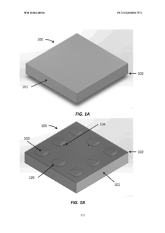
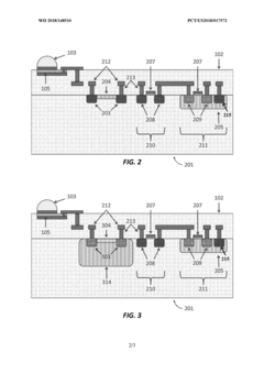
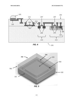
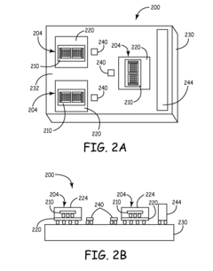
- An integrated MEMS force sensor combining piezoresistive and piezoelectric sensing elements on the same chip, with digital circuitry, where piezoresistive elements measure static forces and piezoelectric elements measure dynamic forces, allowing for improved sensitivity and accuracy by leveraging both signal types.
MEMS sensor with integrated ASIC packaging
PatentInactiveUS20110227173A1
Innovation
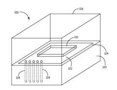
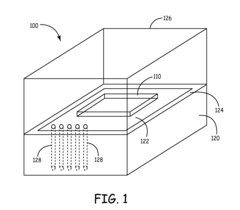
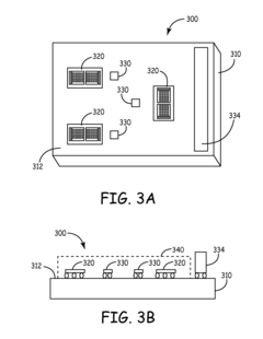
- A sensor assembly comprising a micro-electro-mechanical systems (MEMS) sensor die attached to an integrated circuit (IC) substrate in a stacked configuration, with a seal ring and seal cap for hermetic or vacuum sealing, and the use of thru vias for surface mounting, allowing for integrated electronics and improved sealing techniques.
Fabrication Processes for MEMS-Piezo Devices
The fabrication processes for MEMS-piezo devices involve a complex integration of microfabrication techniques and piezoelectric material deposition. These processes typically begin with the selection of a suitable substrate, often silicon, which serves as the foundation for the device. The substrate undergoes a series of surface preparation steps, including cleaning and oxidation, to ensure optimal adhesion and electrical isolation.
One of the critical steps in MEMS-piezo fabrication is the deposition of the piezoelectric material. Common methods include sputtering, sol-gel deposition, and pulsed laser deposition. Each technique offers unique advantages in terms of film quality, thickness control, and compatibility with other fabrication steps. For instance, sputtering allows for precise control over film composition and thickness, while sol-gel methods offer better conformality and lower processing temperatures.
Following the piezoelectric layer deposition, patterning techniques are employed to define the active areas of the device. Photolithography is widely used, involving the application of photoresist, exposure through a mask, and subsequent development. Etching processes, both wet and dry, are then utilized to remove unwanted material and create the desired device structures. Plasma etching techniques, such as reactive ion etching (RIE), are particularly valuable for achieving high aspect ratio features and precise control over etch profiles.
The integration of electrodes is another crucial aspect of MEMS-piezo device fabrication. Metal deposition techniques, such as evaporation or sputtering, are used to create top and bottom electrodes that interface with the piezoelectric layer. These electrodes must be carefully designed to ensure good electrical contact while minimizing parasitic effects.
Encapsulation and packaging processes are essential for protecting the delicate MEMS structures and ensuring long-term reliability. This may involve the deposition of passivation layers, such as silicon nitride or silicon dioxide, to protect against environmental factors. Wafer bonding techniques are often employed to create hermetically sealed cavities or to integrate the MEMS device with other components.
Throughout the fabrication process, careful consideration must be given to issues such as residual stress management, material compatibility, and thermal budget. Post-processing steps, including annealing and poling of the piezoelectric material, are often necessary to optimize device performance. Advanced fabrication techniques, such as wafer-level packaging and through-silicon via (TSV) technology, are increasingly being adopted to enhance device integration and miniaturization.
Quality control and characterization play a vital role in MEMS-piezo device fabrication. In-line monitoring techniques, such as ellipsometry and X-ray diffraction, are used to assess film properties and ensure process consistency. Final device testing involves electrical, mechanical, and functional characterization to verify performance metrics and yield.
Environmental Impact of MEMS-Piezo Technologies
The integration of piezoelectric sensors in MEMS devices has significant environmental implications that warrant careful consideration. These technologies offer potential benefits in terms of energy efficiency and resource conservation, but also present challenges related to material usage and end-of-life management.
One of the primary environmental advantages of MEMS-piezo technologies is their potential for energy harvesting. By converting mechanical vibrations into electrical energy, these devices can reduce reliance on traditional power sources, potentially lowering overall energy consumption and associated carbon emissions. This is particularly relevant in applications such as wireless sensor networks, where self-powered devices can operate autonomously for extended periods without battery replacements.
However, the manufacturing process of MEMS devices with integrated piezoelectric sensors involves the use of specialized materials, some of which may have environmental concerns. For instance, lead zirconate titanate (PZT), a commonly used piezoelectric material, contains lead, which is toxic and subject to environmental regulations. The industry is actively researching lead-free alternatives, such as potassium sodium niobate (KNN) and bismuth sodium titanate (BNT), to mitigate these concerns.
The miniaturization inherent in MEMS technology contributes to resource efficiency by reducing material consumption. This can lead to a smaller environmental footprint in terms of raw material extraction and processing. Additionally, the compact size of MEMS-piezo devices often results in reduced energy requirements for transportation and storage throughout the supply chain.
End-of-life considerations are crucial for assessing the overall environmental impact of MEMS-piezo technologies. The complex integration of multiple materials in these devices can make recycling challenging. Developing effective recycling processes for recovering valuable materials, such as rare earth elements often used in piezoelectric components, is an area of ongoing research and development.
The durability and longevity of MEMS-piezo devices also play a role in their environmental impact. While these devices are generally designed for long-term operation, factors such as material fatigue and environmental stresses can affect their lifespan. Improving the durability of these devices can reduce the frequency of replacements and associated waste generation.
In applications such as environmental monitoring, MEMS-piezo sensors can contribute to more efficient resource management and pollution control. By enabling real-time, high-resolution data collection, these technologies support informed decision-making in areas like water quality management, air pollution monitoring, and ecosystem preservation.
As the adoption of MEMS-piezo technologies continues to grow, it is essential to conduct comprehensive life cycle assessments to fully understand and optimize their environmental impact. This includes considering the entire product lifecycle, from raw material extraction to manufacturing, use, and eventual disposal or recycling.
Unlock deeper insights with Patsnap Eureka Quick Research — get a full tech report to explore trends and direct your research. Try now!
Generate Your Research Report Instantly with AI Agent
Supercharge your innovation with Patsnap Eureka AI Agent Platform!
