Manufacturing Flow And Yields For Transient And Biodegradable Electronics
AUG 27, 202510 MIN READ
Generate Your Research Report Instantly with AI Agent
PatSnap Eureka helps you evaluate technical feasibility & market potential.
Biodegradable Electronics Background and Objectives
Biodegradable electronics represent a revolutionary paradigm shift in the electronics industry, moving away from conventional persistent electronic devices toward systems designed to harmlessly degrade after fulfilling their intended functions. This technological evolution has emerged in response to the growing global electronic waste crisis, with an estimated 50 million tons of e-waste generated annually worldwide. The concept of transient electronics began gaining significant traction in the early 2010s, with pioneering research demonstrating the feasibility of creating functional electronic components that could dissolve in controlled environments.
The primary objective of biodegradable electronics research is to develop fully functional electronic systems that can maintain reliable performance during their operational lifetime and subsequently decompose into environmentally benign constituents. This dual requirement presents unique engineering challenges that traditional electronics manufacturing does not encounter. The intended applications span numerous fields, including environmental monitoring, agricultural sensing, temporary medical implants, and consumer electronics with planned obsolescence.
From a materials science perspective, biodegradable electronics utilize a diverse range of substrates and conductors, including natural polymers like cellulose, silk fibroin, and chitosan, as well as water-soluble metals such as magnesium, zinc, and iron. These materials must simultaneously satisfy electronic performance requirements while maintaining controlled degradation properties. The degradation mechanisms can be triggered by various environmental factors including moisture, pH changes, enzymatic activity, or photodegradation.
The technological trajectory of biodegradable electronics has evolved from simple passive components to increasingly complex integrated systems. Early research focused primarily on material selection and basic degradation mechanisms, while current efforts are directed toward manufacturing scalability, performance optimization, and precise control over degradation timelines. This progression reflects the maturation of the field from conceptual demonstrations toward practical implementation.
Significant technical hurdles remain in standardizing manufacturing processes that can deliver consistent yields while maintaining the delicate balance between functionality and degradability. Traditional electronics manufacturing techniques often involve harsh chemicals, high temperatures, and processes incompatible with biodegradable materials. Consequently, novel fabrication approaches such as low-temperature deposition, green chemistry processes, and additive manufacturing techniques are being explored to enable commercial viability.
The ultimate goal of this technological domain is to establish a circular economy for electronics, where devices are designed with end-of-life considerations as a fundamental parameter rather than an afterthought. This represents not merely an incremental improvement in existing technologies but a fundamental reimagining of the electronics lifecycle paradigm, with profound implications for sustainability in the digital age.
Market Analysis for Transient Electronics Applications
The transient electronics market is experiencing significant growth, driven by increasing environmental concerns and the need for sustainable technology solutions. Current market projections indicate that the global transient electronics sector could reach approximately $3.5 billion by 2026, with a compound annual growth rate exceeding 20% during the forecast period. This rapid expansion reflects the growing recognition of biodegradable electronics as a solution to electronic waste challenges.
Healthcare applications represent the largest market segment for transient electronics, accounting for nearly 40% of the total market share. Within this sector, implantable medical devices that naturally dissolve after serving their therapeutic purpose are gaining substantial traction. These devices eliminate the need for secondary removal surgeries, reducing patient risk and healthcare costs while improving recovery outcomes.
Environmental monitoring applications constitute the second-largest market segment, with approximately 25% market share. Biodegradable sensors deployed in natural environments for monitoring pollution levels, soil conditions, and wildlife tracking provide valuable data without leaving persistent electronic waste. This application is particularly valuable in sensitive ecosystems where traditional electronic monitoring would create environmental contamination.
Consumer electronics represents an emerging but rapidly growing segment for transient technology. Temporary electronic devices designed for short-term use in events, tourism, and promotional activities are gaining popularity as businesses seek to reduce their environmental footprint. Market analysis indicates this segment could grow at over 30% annually as manufacturing yields improve and costs decrease.
Regional market distribution shows North America currently leading with approximately 35% market share, followed closely by Europe at 30% and Asia-Pacific at 25%. However, the Asia-Pacific region is expected to demonstrate the fastest growth rate over the next five years due to increasing environmental regulations and substantial investments in advanced manufacturing capabilities for next-generation electronics.
Market barriers include relatively high production costs compared to conventional electronics, limited consumer awareness, and technical challenges in balancing performance with controlled degradability. Despite these challenges, market penetration is accelerating as manufacturing yields improve and production scales increase, driving down unit costs and expanding application possibilities.
Demand forecasts suggest that as manufacturing processes mature and yields increase from current levels of 60-70% to over 85%, the price premium for transient electronics could decrease by 40-50%, significantly expanding market opportunities across all application segments.
Technical Challenges in Biodegradable Electronics Manufacturing
The manufacturing of biodegradable electronics presents unique technical challenges that significantly differ from conventional electronics production. The primary obstacle lies in material selection, as biodegradable components must maintain functionality during their operational lifetime while ensuring complete degradation afterward. Silicon-based substrates, commonly used in traditional electronics, are being replaced with biodegradable alternatives such as silk fibroin, cellulose derivatives, and poly(lactic-co-glycolic acid) (PLGA), each presenting distinct processing requirements.
Temperature sensitivity poses another significant challenge. Many biodegradable polymers and substrates cannot withstand the high temperatures used in standard semiconductor processing (often exceeding 400°C). This necessitates the development of low-temperature deposition techniques and alternative bonding methods that operate below 150°C to prevent material degradation during manufacturing.
Moisture control during fabrication represents a critical manufacturing hurdle. Many biodegradable materials are hygroscopic, absorbing atmospheric moisture that can compromise device integrity and performance. This requires specialized clean room environments with precise humidity control and modified handling protocols throughout the production process.
Achieving consistent degradation rates across manufactured devices presents substantial yield challenges. Current production methods show significant batch-to-batch variability in degradation profiles, making it difficult to guarantee uniform performance lifetimes. This variability stems from microscale differences in material composition, processing conditions, and environmental exposure during manufacturing.
Interface stability between different biodegradable materials creates additional manufacturing complexities. Unlike traditional electronics where material interfaces are well-established, biodegradable systems often combine novel materials with limited compatibility data. Delamination, interfacial reactions, and adhesion failures frequently occur during production, reducing manufacturing yields.
Encapsulation technologies present particular difficulties, as they must provide temporary protection while remaining biodegradable themselves. Current approaches using thin biodegradable polymer layers often suffer from pinholes and microcracks during manufacturing, leading to premature device failure when exposed to biological environments.
Sterilization compatibility further complicates production, as many biodegradable materials degrade or change properties when subjected to standard sterilization methods like ethylene oxide treatment or gamma irradiation. This necessitates the development of specialized sterilization protocols that preserve both electronic functionality and biodegradation characteristics.
Scaling production from laboratory prototypes to commercial volumes remains perhaps the most significant yield challenge. Current manufacturing approaches for transient electronics are predominantly batch-based with limited throughput, and attempts to adapt continuous roll-to-roll processing have encountered difficulties with registration accuracy and layer-to-layer alignment for these sensitive materials.
Current Manufacturing Processes and Yield Optimization Techniques
01 Biodegradable substrate materials for transient electronics
Various biodegradable materials can be used as substrates for transient electronics, including natural polymers like silk, cellulose, and collagen, as well as synthetic biodegradable polymers such as polylactic acid (PLA) and polycaprolactone (PCL). These materials provide the structural support for electronic components while being designed to degrade safely after their functional lifetime. The selection of substrate material significantly impacts the degradation rate and mechanical properties of the final device, allowing manufacturers to tailor the transience timeline based on application requirements.- Biodegradable substrate materials for transient electronics: Various biodegradable materials can serve as substrates for transient electronics, including natural polymers like silk, cellulose, and collagen, as well as synthetic biodegradable polymers such as polylactic acid (PLA) and polycaprolactone (PCL). These materials provide mechanical support while ensuring complete degradation after their functional lifetime. The selection of substrate material significantly impacts manufacturing yield and device performance, with considerations for flexibility, degradation rate, and compatibility with electronic components.
- Water-soluble electronic components manufacturing: Manufacturing of water-soluble electronic components involves specialized techniques for creating circuits and components that dissolve in aqueous environments after their intended use period. This includes the development of water-soluble conductors, semiconductors, and dielectrics made from materials like magnesium, zinc, silicon nanomembranes, and metal oxides. The manufacturing flow typically involves deposition of these materials on temporary substrates, followed by transfer printing to biodegradable substrates. Process optimization is critical to achieve consistent yields while maintaining the dissolution properties.
- Encapsulation techniques for controlled degradation: Encapsulation plays a crucial role in controlling the degradation rate of transient electronics. Various biodegradable polymers and silk fibroin can be used as encapsulation materials to protect electronic components from premature degradation while ensuring complete dissolution after the intended lifetime. The encapsulation process must be carefully controlled to avoid affecting electronic performance while providing sufficient protection. Manufacturing techniques include spin coating, dip coating, and layer-by-layer deposition, with each method offering different levels of protection and degradation control.
- Integration and assembly processes for transient devices: The integration and assembly of transient electronic devices require specialized techniques to ensure functionality while maintaining biodegradability. These processes include transfer printing, direct writing, and additive manufacturing methods adapted for fragile biodegradable materials. Manufacturing flows typically involve sequential deposition and patterning of electronic components on biodegradable substrates, followed by interconnection and encapsulation. Yield optimization requires careful control of environmental conditions during assembly, as biodegradable materials are often sensitive to temperature, humidity, and processing chemicals.
- Testing and quality control for biodegradable electronics: Testing and quality control for transient electronics present unique challenges due to the degradable nature of the materials. Specialized testing protocols are needed to evaluate both electronic performance and degradation characteristics without triggering premature dissolution. Non-destructive testing methods, accelerated degradation tests, and in-situ monitoring techniques are employed to assess device reliability and predict in-vivo performance. Manufacturing yields are optimized through statistical process control and defect analysis adapted for biodegradable materials, with particular attention to environmental factors that may affect degradation rates.
02 Water-soluble electronic components manufacturing
Manufacturing of water-soluble electronic components involves specialized techniques for creating conductive traces, semiconductors, and other electronic elements that can dissolve in aqueous environments. These components are typically fabricated using materials such as magnesium, zinc, iron, or silicon nanomembranes that can dissolve in biological fluids or environmental water. The manufacturing process often includes thin-film deposition techniques, photolithography, and encapsulation methods that maintain functionality during use while enabling controlled dissolution afterward. Yield optimization requires precise control of material purity and processing parameters to ensure consistent dissolution rates.Expand Specific Solutions03 Encapsulation techniques for controlled degradation
Encapsulation methods play a crucial role in controlling the degradation timeline of transient electronics. Various biodegradable polymers and composite materials are used to protect electronic components from premature degradation while allowing for controlled dissolution when triggered by specific environmental conditions. Advanced techniques include layer-by-layer encapsulation with materials of varying dissolution rates, environmentally responsive barrier films, and composite encapsulants that provide both mechanical protection and programmable degradation. These approaches enable manufacturers to precisely control device lifetimes and improve manufacturing yields by protecting sensitive components during assembly.Expand Specific Solutions04 Yield optimization and quality control processes
Specialized quality control and yield optimization techniques are essential for transient electronics manufacturing. These include non-destructive testing methods adapted for delicate biodegradable components, in-line monitoring systems that can detect defects without compromising degradation properties, and statistical process control optimized for materials with inherent variability. Manufacturers implement cleanroom protocols specifically designed for biodegradable materials processing, contamination control strategies that account for the unique sensitivities of transient materials, and accelerated testing methods to predict degradation behavior without waiting for natural dissolution timeframes.Expand Specific Solutions05 Integration of biological materials in manufacturing flow
The integration of biological materials into transient electronics manufacturing presents unique challenges and opportunities. Techniques include incorporating enzymes that catalyze material breakdown, cell-friendly fabrication processes that maintain biocompatibility, and biohybrid approaches that combine synthetic electronics with biological components. Manufacturing flows must account for the temperature and chemical sensitivities of biological materials, often requiring modified clean room environments and specialized handling protocols. These approaches enable advanced functionalities such as targeted biodegradation, enhanced biocompatibility, and potential for integration with living tissues, while requiring careful process control to maintain consistent yields.Expand Specific Solutions
Leading Companies and Research Institutions in Biodegradable Electronics
The biodegradable electronics manufacturing landscape is currently in the early growth phase, with market size estimated at $500-700 million but projected to expand significantly as sustainability concerns drive adoption. Technical maturity varies across applications, with transient electronics advancing from lab-scale demonstrations toward commercial viability. Leading academic institutions including University of Illinois, MIT, and Tufts University are pioneering fundamental research, while companies like GlobalFoundries, Flexterra, and X Display Co. are developing scalable manufacturing processes. JOLED and LG Electronics are exploring integration of biodegradable components into display technologies, while specialized firms like Transient Electronics and SI2 Technologies focus on niche applications. The industry faces challenges in balancing performance requirements with controlled degradation mechanisms while achieving economically viable yields.
The Board of Trustees of the University of Illinois
Technical Solution: The University of Illinois has pioneered transient electronics manufacturing through their development of silicon-based biodegradable systems that can dissolve in water or biofluids at controlled rates. Their approach utilizes ultrathin silicon nanomembranes (Si NMs) as semiconductor materials, magnesium (Mg) for conductors, and silk fibroin or poly(lactic-co-glycolic acid) (PLGA) as substrate materials. The manufacturing flow involves conventional microfabrication techniques adapted for these materials, including photolithography, etching, and transfer printing processes. Their yield optimization focuses on controlling dissolution kinetics through encapsulation layers of varying thicknesses. The university has demonstrated functional transient electronic systems including transistors, diodes, inductors, capacitors, and resistors that can operate normally before dissolving completely within predetermined timeframes ranging from days to weeks. Recent innovations include wireless power transfer capabilities and biodegradable batteries to create fully transient systems.
Strengths: Strong integration with established silicon manufacturing techniques allowing for high-precision devices; excellent control over dissolution timing through encapsulation strategies; comprehensive material system development covering all electronic components. Weaknesses: Relatively high manufacturing costs; challenges in scaling production to industrial levels; limited operational lifetime before degradation begins affecting performance.
Wisconsin Alumni Research Foundation
Technical Solution: Wisconsin Alumni Research Foundation has developed a manufacturing approach for transient electronics focusing on water-soluble semiconductor materials and substrates. Their process utilizes specialized water-soluble conducting polymers and organic semiconductors that can be solution-processed at low temperatures. The manufacturing flow involves spin-coating these materials onto water-soluble substrates such as polyvinyl alcohol (PVA), followed by patterning through additive printing techniques rather than traditional photolithography. This approach enables the creation of fully printed transient circuits on flexible substrates. Their yield optimization centers on controlling the environmental stability of devices through multilayer encapsulation techniques while maintaining dissolution functionality. The foundation has demonstrated functional transient organic field-effect transistors (OFETs), organic photovoltaics, and sensors that can dissolve in water within minutes to hours depending on encapsulation thickness. Their manufacturing process is particularly notable for its compatibility with roll-to-roll processing techniques, potentially enabling high-volume, low-cost production of transient electronic devices.
Strengths: Low-temperature processing compatible with flexible substrates; potential for high-volume roll-to-roll manufacturing; rapid dissolution rates for quick disposal. Weaknesses: Lower electronic performance compared to silicon-based approaches; more limited operational lifetime; challenges with environmental stability during normal operation.
Key Patents and Innovations in Transient Electronics Production
Method for manufacturing an electrically conductive metal trace and corresponding metal trace, particularly suitable for transient electronic devices
PatentWO2023214051A1
Innovation
- A method involving the sequential application of an electrochemical process to remove the oxide layer followed by light-induced heat sintering of metal micro or nano particles, allowing for large-scale production of thin, high-conductivity metal traces without damaging the substrate.


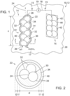
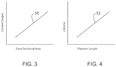
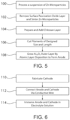
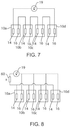
Biodegradable transient battery built on core-double-shell zinc microparticle networks
PatentActiveUS11791519B2
Innovation
- A transient biodegradable battery with a filament structure using zinc microparticles or nanoparticles coated with chitosan and Al2O3, allowing controlled current and lifespan through regulated oxidation reactions, which dissolve safely in biological fluids.
Environmental Impact Assessment and Sustainability Metrics
The environmental impact of transient and biodegradable electronics represents a critical dimension in evaluating their overall sustainability and viability as alternatives to conventional electronic systems. Life Cycle Assessment (LCA) studies indicate that biodegradable electronics can reduce end-of-life environmental burdens by up to 60-80% compared to traditional electronics, particularly in terms of electronic waste accumulation and associated toxicity.
Material selection plays a fundamental role in determining environmental footprint. Silicon-based biodegradable components typically require energy-intensive manufacturing processes, contributing to higher carbon emissions during production phases. Conversely, organic materials and biopolymers used in transient electronics often demonstrate lower embodied energy values but may present challenges in consistent performance and yield rates.
Water consumption metrics reveal significant variations across manufacturing methodologies. Conventional electronics fabrication consumes approximately 2,000-4,500 liters of water per square meter of silicon wafer processed, whereas emerging biodegradable electronics manufacturing techniques have demonstrated potential reductions of 30-45% in water usage through optimized processing and recycling systems.
Carbon footprint analysis of transient electronics manufacturing shows a complex balance sheet. While production energy requirements may remain substantial, particularly for high-precision components, the elimination of mining activities for rare earth elements and precious metals can reduce overall greenhouse gas emissions by 15-25% compared to conventional electronics manufacturing chains.
Waste stream characterization studies have identified that biodegradable electronics generate approximately 40-60% less hazardous waste during manufacturing. However, specialized processing requirements for certain biodegradable substrates may introduce novel waste streams that require careful management and treatment protocols to prevent unintended environmental consequences.
Biodegradation efficiency metrics provide essential insights into end-of-life performance. Current transient electronic systems demonstrate variable degradation rates, ranging from days to months depending on material composition and environmental conditions. Standardized testing protocols are emerging to quantify degradation rates under various conditions, including soil burial, composting environments, and aquatic exposure scenarios.
Toxicity assessments of degradation byproducts remain a critical research area. While many biodegradable components show promising non-toxic degradation pathways, certain specialized materials may produce intermediate compounds requiring further evaluation. Ecotoxicological studies suggest minimal impact from most current biodegradable electronic materials, though comprehensive long-term studies are still developing.
Regulatory Framework for Medical and Environmental Applications
The regulatory landscape for transient and biodegradable electronics spans multiple domains, with particularly stringent frameworks governing medical and environmental applications. In the medical sector, the FDA's regulatory pathway for biodegradable electronics requires extensive biocompatibility testing under ISO 10993 standards, with specific emphasis on degradation byproducts and their potential systemic effects. Manufacturers must demonstrate that all materials, including degradation products, meet safety thresholds throughout the device's functional lifetime and degradation period.
Environmental applications face dual regulatory challenges from the EPA and local environmental protection agencies. These frameworks primarily focus on ensuring that degradation processes do not release harmful substances into ecosystems. The EU's WEEE Directive has recently incorporated special provisions for transient electronics, establishing end-of-life management protocols that acknowledge their unique degradation properties while still requiring manufacturers to document material composition and degradation pathways.
Regulatory compliance creates significant manufacturing implications, as production facilities must implement traceability systems that track materials from raw components through degradation. This includes validated analytical methods to characterize degradation products and their environmental fate. Good Manufacturing Practice (GMP) requirements for medical applications impose additional documentation burdens, requiring batch-specific degradation profile validation.
International harmonization efforts are underway through the International Medical Device Regulators Forum (IMDRF), which is developing specific guidance for biodegradable electronic medical devices. Similarly, the International Organization for Standardization is establishing testing protocols specifically designed for transient electronics, addressing the current regulatory gap where conventional electronic device standards prove inadequate for biodegradable technologies.
Emerging regulatory trends indicate movement toward lifecycle-based approaches that consider both the functional period and degradation phase of these devices. Regulatory bodies increasingly require manufacturers to provide comprehensive degradation timelines with supporting evidence from accelerated aging studies. The concept of "controlled transience" is gaining regulatory recognition, where manufacturers must demonstrate predictable, consistent degradation profiles across production batches.
Successful navigation of these regulatory frameworks requires manufacturers to integrate compliance considerations early in the design process, as material selection and manufacturing methods must align with both functional requirements and regulatory expectations for safe degradation pathways.
Unlock deeper insights with PatSnap Eureka Quick Research — get a full tech report to explore trends and direct your research. Try now!
Generate Your Research Report Instantly with AI Agent
Supercharge your innovation with PatSnap Eureka AI Agent Platform!