Miniaturization Challenges in Piezoelectric Sensors
JUL 17, 20259 MIN READ
Generate Your Research Report Instantly with AI Agent
Patsnap Eureka helps you evaluate technical feasibility & market potential.
Piezoelectric Sensor Miniaturization Background
Piezoelectric sensors have been a cornerstone of sensing technology for decades, offering unique capabilities in converting mechanical stress into electrical signals. The drive towards miniaturization in this field has been fueled by the increasing demand for compact, high-performance sensing solutions across various industries. This trend aligns with the broader movement towards smaller, more efficient electronic devices and systems.
The journey of piezoelectric sensor miniaturization began in the mid-20th century, with early applications primarily in sonar and ultrasound technologies. As manufacturing processes improved, particularly in thin-film deposition and microfabrication techniques, the ability to create smaller piezoelectric elements became feasible. This progression has been marked by significant milestones, including the development of MEMS (Micro-Electro-Mechanical Systems) based piezoelectric sensors in the 1990s, which dramatically reduced sensor size while maintaining or even improving performance.
The evolution of piezoelectric materials has played a crucial role in this miniaturization process. Traditional bulk piezoelectric materials like quartz and lead zirconate titanate (PZT) have given way to advanced thin-film piezoelectric materials such as aluminum nitride (AlN) and zinc oxide (ZnO). These materials offer superior performance in microscale applications, enabling the creation of sensors with dimensions in the micrometer range.
Miniaturization efforts have been driven by several key technological goals. These include increasing sensitivity and resolution, reducing power consumption, improving frequency response, and enhancing integration capabilities with other electronic components. The pursuit of these objectives has led to innovative designs and fabrication methods, such as the use of nanostructures and composite materials to enhance piezoelectric properties at smaller scales.
However, the path to miniaturization has not been without challenges. As sensors become smaller, issues such as reduced output signal, increased noise susceptibility, and thermal management become more pronounced. Engineers and researchers have had to develop novel solutions to overcome these obstacles, including advanced signal processing techniques, improved shielding methods, and the use of new materials with enhanced piezoelectric coefficients.
The ongoing miniaturization of piezoelectric sensors is closely tied to advancements in related fields such as nanotechnology, materials science, and microfabrication. This interdisciplinary approach has been crucial in pushing the boundaries of what is possible in sensor design and performance. As we look towards the future, the continued miniaturization of piezoelectric sensors promises to enable new applications in areas such as wearable technology, biomedical implants, and the Internet of Things (IoT), where size, power efficiency, and performance are critical factors.
Market Demand Analysis
The market demand for miniaturized piezoelectric sensors has been steadily increasing across various industries, driven by the growing need for compact, high-performance sensing solutions. This trend is particularly evident in sectors such as healthcare, consumer electronics, automotive, and industrial automation.
In the healthcare industry, there is a significant demand for miniaturized piezoelectric sensors in wearable medical devices and implantable medical technologies. These sensors enable continuous health monitoring, early disease detection, and personalized treatment options. The global wearable medical devices market is expected to experience substantial growth, creating opportunities for miniaturized piezoelectric sensors.
The consumer electronics sector represents another major market for miniaturized piezoelectric sensors. With the proliferation of smartphones, smartwatches, and other portable devices, manufacturers are constantly seeking ways to incorporate more functionality into smaller form factors. Miniaturized piezoelectric sensors play a crucial role in enabling features such as haptic feedback, gesture recognition, and pressure-sensitive interfaces.
In the automotive industry, the demand for miniaturized piezoelectric sensors is driven by the increasing adoption of advanced driver assistance systems (ADAS) and the development of autonomous vehicles. These sensors are essential for applications such as tire pressure monitoring, engine knock detection, and structural health monitoring of vehicle components.
The industrial automation sector is also experiencing a growing demand for miniaturized piezoelectric sensors. These sensors are used in various applications, including vibration monitoring, process control, and quality assurance. The trend towards Industry 4.0 and smart manufacturing is expected to further boost the demand for compact, high-precision sensing solutions.
Market analysts predict a compound annual growth rate (CAGR) for the piezoelectric sensors market in the coming years, with miniaturization being a key driver of this growth. The ability to produce smaller, more efficient sensors is expected to open up new application areas and market opportunities.
However, the market demand for miniaturized piezoelectric sensors also presents several challenges. Manufacturers must balance the need for smaller form factors with maintaining or improving sensor performance. Additionally, cost considerations play a significant role in market adoption, particularly in price-sensitive industries.
As the demand for miniaturized piezoelectric sensors continues to grow, there is an increasing focus on developing new materials and manufacturing techniques to overcome current limitations. This includes research into novel piezoelectric materials with improved properties and advanced fabrication methods that enable the production of smaller, more precise sensors.
Current Challenges
The miniaturization of piezoelectric sensors presents several significant challenges that researchers and engineers are currently grappling with. One of the primary obstacles is maintaining sensor performance while reducing size. As sensors become smaller, their sensitivity and signal-to-noise ratio tend to decrease, potentially compromising the accuracy and reliability of measurements. This issue is particularly pronounced in applications requiring high precision, such as medical devices or aerospace systems.
Another critical challenge lies in the fabrication processes for miniaturized piezoelectric sensors. Traditional manufacturing techniques may not be suitable for producing extremely small components with the necessary precision. Advanced microfabrication methods, such as photolithography and etching, are being explored but often require substantial investment in equipment and expertise. Additionally, ensuring consistent quality and reproducibility at microscale levels remains a significant hurdle.
The integration of miniaturized piezoelectric sensors into larger systems poses its own set of challenges. As sensors shrink, issues related to electrical connections, packaging, and environmental protection become more complex. Designers must find innovative ways to interface these tiny sensors with standard electronic components and protect them from external factors like moisture, temperature fluctuations, and mechanical stress, all while maintaining the compact form factor.
Power management is another area of concern in the miniaturization of piezoelectric sensors. Smaller sensors typically generate less electrical output, which can be problematic for energy harvesting applications or self-powered systems. Engineers are exploring novel circuit designs and energy storage solutions to address this limitation, but finding the right balance between power generation, consumption, and overall device size remains challenging.
Material selection and optimization present additional hurdles in sensor miniaturization. While traditional piezoelectric materials like lead zirconate titanate (PZT) offer excellent performance, they may not be ideal for all miniaturized applications due to their brittleness or environmental concerns. Researchers are investigating alternative materials, including flexible piezoelectric polymers and nanocomposites, but these often come with trade-offs in terms of piezoelectric coefficients or temperature stability.
Lastly, the characterization and testing of miniaturized piezoelectric sensors pose unique challenges. Conventional measurement techniques may not be suitable for evaluating the performance of microscale devices. Developing new metrology tools and standardized testing protocols for these tiny sensors is crucial for ensuring their reliability and comparability across different applications and manufacturers.
Existing Solutions
01 Miniaturization of piezoelectric sensors
Advancements in manufacturing techniques have led to the development of smaller piezoelectric sensors. These miniaturized sensors maintain high sensitivity while reducing overall device size, making them suitable for applications where space is limited. The reduced size also allows for integration into compact electronic devices and wearable technology.- Miniaturization of piezoelectric sensors: Advancements in manufacturing techniques have led to the development of smaller piezoelectric sensors. These miniaturized sensors maintain high sensitivity while reducing overall device size, making them suitable for applications where space is limited. The reduced size also allows for integration into compact electronic devices and microelectromechanical systems (MEMS).
- Nanostructured piezoelectric materials: Utilizing nanostructured materials in piezoelectric sensors has enabled the creation of ultra-small sensing elements. These nanostructures, such as nanowires or nanoparticles, offer improved performance in terms of sensitivity and response time while significantly reducing the overall sensor size. This approach allows for the development of highly efficient, compact piezoelectric sensors.
- Thin-film piezoelectric sensors: Thin-film technology has been applied to create extremely thin piezoelectric sensors. These sensors can be fabricated with thicknesses in the range of nanometers to micrometers, allowing for seamless integration into various devices and structures. The reduced thickness contributes to overall size reduction while maintaining sensor functionality.
- Array-based piezoelectric sensor designs: Implementing array-based designs for piezoelectric sensors allows for increased functionality within a compact form factor. These arrays consist of multiple small sensing elements arranged in a specific pattern, enabling multi-point or distributed sensing capabilities. This approach optimizes space utilization while enhancing the sensor's overall performance and versatility.
- Flexible and stretchable piezoelectric sensors: Development of flexible and stretchable piezoelectric sensors has led to ultra-thin, conformable designs. These sensors can be fabricated using innovative materials and structures that allow them to bend, stretch, and adapt to various surfaces. The flexibility and stretchability contribute to size reduction by eliminating the need for rigid, bulky components while enabling new applications in wearable technology and soft robotics.
02 Nanostructured piezoelectric materials
Utilizing nanostructured materials in piezoelectric sensors has enabled the creation of ultra-small sensing elements. These nanostructures, such as nanowires or nanoparticles, offer improved performance in terms of sensitivity and response time while significantly reducing the overall sensor size. This approach allows for the development of highly compact and efficient piezoelectric sensors.Expand Specific Solutions03 MEMS-based piezoelectric sensors
Micro-Electro-Mechanical Systems (MEMS) technology has been applied to piezoelectric sensors, resulting in extremely small form factors. These MEMS-based sensors integrate piezoelectric materials with microfabrication techniques to create miniature sensing devices. The reduced size of MEMS piezoelectric sensors makes them ideal for applications in microfluidics, biomedical devices, and other space-constrained environments.Expand Specific Solutions04 Flexible and thin-film piezoelectric sensors
Development of flexible and thin-film piezoelectric sensors has led to a significant reduction in sensor thickness. These sensors can be as thin as a few micrometers while maintaining their sensing capabilities. The flexibility and thinness of these sensors make them suitable for integration into wearable devices, smart textiles, and conformable electronics.Expand Specific Solutions05 Array-based miniature piezoelectric sensors
Arranging multiple small piezoelectric sensing elements in an array format has enabled the creation of compact multi-point sensing systems. These arrays can provide high-resolution spatial sensing while maintaining a small overall footprint. This approach is particularly useful in applications such as tactile sensing, pressure mapping, and acoustic imaging where multiple sensing points are required in a limited space.Expand Specific Solutions
Key Industry Players
The miniaturization of piezoelectric sensors is currently in a competitive and rapidly evolving phase. The market is experiencing significant growth, driven by increasing demand for compact, high-performance sensors across various industries. Key players like Murata Manufacturing, Seiko Epson, and Kyocera are leading the field, leveraging their expertise in fine ceramics and electronic components. The technology is approaching maturity, with companies like Texas Instruments and Bosch pushing boundaries in sensor miniaturization. Universities and research institutions, such as Chongqing University and Fraunhofer-Gesellschaft, are contributing to advancements through collaborative research efforts. As the market expands, we're seeing increased competition from emerging players like BOE Technology Group, focusing on innovative applications in IoT and smart devices.
Murata Manufacturing Co. Ltd.
Technical Solution: Murata has developed advanced MEMS-based piezoelectric sensors to address miniaturization challenges. Their approach involves using thin-film piezoelectric materials, such as aluminum nitride (AlN) or lead zirconate titanate (PZT), deposited on silicon wafers. This allows for the creation of ultra-compact sensors with dimensions as small as 1.0 x 0.8 x 0.6 mm[1]. Murata's sensors incorporate innovative electrode designs and packaging techniques to maintain high sensitivity and performance despite their reduced size. They have also implemented wafer-level packaging (WLP) technology to further minimize the overall sensor footprint[2].
Strengths: Industry-leading miniaturization capabilities, high-volume production expertise, and advanced MEMS fabrication techniques. Weaknesses: Potential trade-offs between size reduction and sensor performance, higher production costs for ultra-miniature devices.
Seiko Epson Corp.
Technical Solution: Seiko Epson has developed proprietary QMEMS (Quartz MEMS) technology to address miniaturization challenges in piezoelectric sensors. This approach combines the high precision of quartz with MEMS manufacturing techniques. Epson's QMEMS sensors utilize photolithography and deep reactive ion etching (DRIE) to create miniaturized quartz structures with precise dimensions and high aspect ratios[3]. The company has achieved sensor sizes down to 2.0 x 1.6 x 0.5 mm while maintaining excellent frequency stability and temperature characteristics. Epson has also implemented innovative packaging solutions, such as wafer-level chip scale packaging (WLCSP), to further reduce the overall sensor size[4].
Strengths: Unique QMEMS technology combining quartz precision with MEMS scalability, excellent frequency stability in miniaturized form factors. Weaknesses: Limited to quartz-based sensors, potentially higher production costs compared to silicon-based MEMS.
Core Innovations
Piezoelectric element and piezoelectric sensor
PatentWO2015041016A1
Innovation
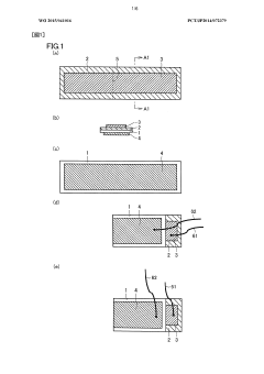
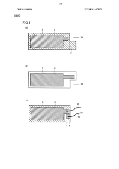
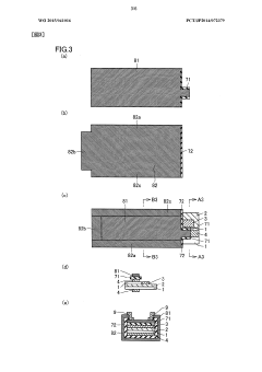
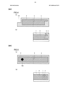
- A piezoelectric element is formed by bending a laminate with a piezoelectric layer sandwiched between insulating and electrode layers, where both electrode layers are exposed on one surface, allowing for single-sided cable connection and reduced part count, using a flexible insulating film and conductive layers to enhance shielding and reduce manufacturing complexity.
Piezoelectrical device for measuring impulses
PatentInactiveEP1300663A2
Innovation
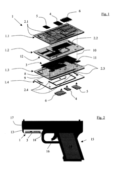
- The piezo film sensor is fully integrated between the layers of a multi-layer circuit board, maximizing its surface area to withstand mechanical deformations and protect it from damage, while maintaining sensitivity through strategic recesses and connections.
Material Advancements
Material advancements play a crucial role in addressing the miniaturization challenges faced by piezoelectric sensors. As the demand for smaller, more efficient sensors grows across various industries, researchers and engineers are exploring innovative materials to overcome the limitations of traditional piezoelectric materials.
One significant area of development is the exploration of nanostructured materials. These materials, such as nanowires, nanotubes, and nanoparticles, offer unique properties that can enhance the performance of miniaturized piezoelectric sensors. For instance, zinc oxide nanowires have shown promising results in generating higher piezoelectric responses compared to their bulk counterparts, allowing for more sensitive and compact sensor designs.
Another avenue of material advancement is the development of composite materials. By combining different piezoelectric materials or integrating piezoelectric materials with other functional materials, researchers can create sensors with improved sensitivity and reduced size. For example, polymer-ceramic composites have gained attention due to their flexibility and ability to be fabricated into thin films, making them ideal for miniaturized sensor applications.
The emergence of two-dimensional materials, such as graphene and transition metal dichalcogenides, has opened up new possibilities for ultra-thin piezoelectric sensors. These materials exhibit unique piezoelectric properties at the atomic scale, allowing for the development of sensors with thicknesses of just a few atoms. This breakthrough has the potential to revolutionize the field of miniaturized piezoelectric sensors.
Advancements in ferroelectric materials have also contributed to the miniaturization efforts. Researchers are exploring new compositions and structures of ferroelectric materials that can maintain their piezoelectric properties at smaller scales. This includes the development of relaxor ferroelectrics and domain-engineered crystals, which offer enhanced piezoelectric responses in reduced dimensions.
Furthermore, the integration of smart materials and multifunctional materials is gaining traction in the field of miniaturized piezoelectric sensors. These materials can adapt to their environment or perform multiple functions simultaneously, allowing for more compact and efficient sensor designs. For instance, materials that exhibit both piezoelectric and piezoresistive properties can enable the development of sensors with improved sensitivity and reduced size.
As material science continues to advance, new fabrication techniques and processing methods are being developed to optimize the properties of piezoelectric materials at smaller scales. These include techniques such as atomic layer deposition, epitaxial growth, and precision doping, which allow for greater control over material composition and structure at the nanoscale.
Manufacturing Processes
The manufacturing processes for miniaturized piezoelectric sensors present unique challenges that require innovative approaches and precision engineering. Traditional fabrication methods often struggle to maintain the desired piezoelectric properties when scaling down to micro and nano dimensions. One key process in manufacturing miniaturized piezoelectric sensors is thin film deposition, which can be achieved through various techniques such as sputtering, pulsed laser deposition, or chemical vapor deposition. These methods allow for the creation of ultra-thin piezoelectric layers with controlled composition and crystal structure.
Another critical aspect of the manufacturing process is the patterning and etching of the piezoelectric materials. Photolithography and electron beam lithography are commonly employed to define precise sensor geometries, while wet and dry etching techniques are used to remove excess material and create the desired sensor structures. The choice of etching method significantly impacts the final device performance, as it can affect the surface quality and piezoelectric properties of the material.
Integration of the piezoelectric elements with other components, such as electrodes and substrates, is a crucial step in the manufacturing process. Techniques like wafer bonding, flip-chip bonding, or direct growth of piezoelectric materials on substrates are utilized to achieve seamless integration. These processes must be carefully optimized to ensure good adhesion, electrical contact, and preservation of the piezoelectric properties.
The miniaturization of piezoelectric sensors also necessitates the development of specialized packaging techniques. Hermetic sealing and encapsulation methods are employed to protect the sensitive piezoelectric elements from environmental factors while maintaining their functionality. Advanced packaging solutions, such as through-silicon vias (TSVs) and 3D integration, are being explored to further reduce the overall sensor size and improve performance.
Quality control and characterization play a vital role in the manufacturing process of miniaturized piezoelectric sensors. Non-destructive testing methods, such as X-ray diffraction and atomic force microscopy, are used to assess the crystal structure and surface morphology of the piezoelectric materials. Electrical and mechanical testing, including impedance analysis and displacement measurements, are performed to verify the sensor's performance and reliability.
As the demand for smaller and more sensitive piezoelectric sensors continues to grow, manufacturers are exploring novel fabrication techniques. Additive manufacturing methods, such as 3D printing of piezoelectric materials, show promise for creating complex sensor geometries with reduced material waste. Additionally, bottom-up approaches like self-assembly and template-assisted growth are being investigated for the fabrication of nanostructured piezoelectric sensors with enhanced properties.
Unlock deeper insights with Patsnap Eureka Quick Research — get a full tech report to explore trends and direct your research. Try now!
Generate Your Research Report Instantly with AI Agent
Supercharge your innovation with Patsnap Eureka AI Agent Platform!
