

Optical Wavelength Selection For Maximum PV Conversion Efficiency
AUG 28, 20259 MIN READ
Generate Your Research Report Instantly with AI Agent
Patsnap Eureka helps you evaluate technical feasibility & market potential.
Photovoltaic Technology Evolution and Efficiency Goals
Photovoltaic (PV) technology has undergone remarkable evolution since the discovery of the photovoltaic effect by Alexandre Edmond Becquerel in 1839. The first practical silicon solar cell was developed at Bell Laboratories in 1954 with an efficiency of merely 6%. This milestone marked the beginning of a technological journey that has seen continuous improvements in conversion efficiency, manufacturing processes, and material science.
The evolution of PV technology can be categorized into distinct generations. First-generation cells, based on crystalline silicon wafers, dominated the market for decades and continue to represent approximately 95% of the global PV market. Second-generation thin-film technologies emerged in the 1970s, offering reduced material usage and manufacturing costs, albeit with lower efficiencies. Third-generation technologies, including multi-junction cells, organic photovoltaics, and perovskites, represent the cutting edge of research, promising both higher efficiencies and potentially lower costs.
Efficiency improvements have followed a relatively predictable trajectory, with commercial silicon modules improving from approximately 15% in the early 2000s to over 22% today. Laboratory efficiencies have shown even more impressive gains, with multi-junction concentrator cells achieving over 47% efficiency in controlled settings. This progression demonstrates the industry's commitment to maximizing the conversion of solar radiation into usable electricity.
The strategic goal for PV technology development centers on achieving the theoretical maximum efficiency while maintaining economic viability. The Shockley-Queisser limit establishes a theoretical maximum of approximately 33% for single-junction silicon cells under standard conditions. However, this limit can be circumvented through various approaches, including spectrum splitting, multi-junction architectures, and novel materials that can better utilize the solar spectrum.
Optical wavelength selection represents a critical frontier in this pursuit. The solar spectrum spans from ultraviolet to infrared wavelengths, but conventional PV cells can only efficiently convert a portion of this spectrum into electricity. Silicon cells, for instance, primarily respond to wavelengths between 400-1100 nm, leaving significant portions of the available solar energy untapped. Advanced optical management techniques, including spectral splitting, up/down-conversion, and plasmonic enhancement, aim to better match the absorption characteristics of PV materials to the solar spectrum.
Industry roadmaps and research initiatives have established ambitious efficiency targets. The U.S. Department of Energy's SunShot Initiative aims for utility-scale solar costs of $0.03/kWh by 2030, necessitating continued efficiency improvements. The European Strategic Energy Technology Plan similarly emphasizes the need for higher-efficiency PV technologies to meet renewable energy goals. These targets drive research into optimal wavelength utilization as a key pathway to achieving next-generation PV performance.
Market Analysis of High-Efficiency Solar Cell Demand
The global market for high-efficiency solar cells has experienced remarkable growth over the past decade, driven primarily by increasing environmental concerns, government incentives, and declining manufacturing costs. Current market valuations indicate that the high-efficiency solar cell segment represents approximately 35% of the total photovoltaic market, with annual growth rates consistently exceeding 20% since 2018.
Demand for solar cells with enhanced conversion efficiency is particularly strong in regions with limited installation space, such as Japan, South Korea, and urban centers across Europe and North America. These markets prioritize maximum energy generation per unit area, making optical wavelength optimization technologies especially valuable. Commercial rooftop installations have emerged as a key application segment, where the premium for high-efficiency modules can be more easily justified through improved return on investment calculations.
Utility-scale solar projects are increasingly specifying higher efficiency requirements in their procurement processes. This shift represents a significant market evolution, as large-scale installations traditionally prioritized cost per watt over efficiency metrics. Market research indicates that modules achieving efficiency ratings above 22% command price premiums of 15-30% compared to standard modules, demonstrating strong commercial incentive for optical wavelength optimization technologies.
Geographically, China remains the largest market for high-efficiency solar cells, accounting for approximately 40% of global demand. However, emerging markets in India, Southeast Asia, and Latin America are showing the highest growth rates, with annual demand increases exceeding 30% in these regions. These markets are particularly sensitive to performance improvements that enhance energy yield in challenging climate conditions, such as high temperatures and variable light conditions.
Consumer sentiment analysis reveals increasing awareness and preference for higher efficiency solar products among residential customers. This trend is supported by the growing integration of solar with home energy management systems and electric vehicle charging infrastructure, where maximizing energy production within limited roof space delivers tangible benefits to homeowners.
Industry forecasts project the high-efficiency solar cell market to reach 180 GW annual production capacity by 2025, representing a compound annual growth rate of 25%. Technologies specifically focused on optical wavelength selection and optimization are expected to capture an increasing share of this market, as manufacturers seek competitive differentiation beyond conventional efficiency improvement approaches.
Current Limitations in Optical Wavelength Utilization
Despite significant advancements in photovoltaic (PV) technology, current solar cells face fundamental limitations in their ability to efficiently utilize the full solar spectrum. The spectral mismatch between incoming solar radiation and semiconductor absorption capabilities represents one of the most significant barriers to achieving theoretical maximum conversion efficiencies. Conventional silicon-based solar cells, which dominate the market, can only effectively convert photons with energies close to their bandgap (approximately 1.1 eV), corresponding to wavelengths around 1100 nm.
The Shockley-Queisser limit establishes a theoretical maximum efficiency of about 33% for single-junction solar cells under standard AM1.5G illumination. This limitation stems from three primary loss mechanisms: sub-bandgap losses (photons with insufficient energy pass through the cell without being absorbed), thermalization losses (excess energy from high-energy photons is lost as heat), and recombination losses (electron-hole pairs recombining before extraction).
Current commercial silicon PV modules typically achieve efficiencies between 18-22%, significantly below the theoretical limit. This gap exists partly because silicon, as an indirect bandgap semiconductor, requires greater material thickness for adequate light absorption, increasing recombination probability. Additionally, reflection losses at the cell surface and parasitic absorption in non-active layers further reduce the optical wavelength utilization efficiency.
The spectral response of existing PV technologies is also heavily biased toward visible light, with diminishing conversion capabilities in the infrared and ultraviolet regions. This creates a substantial mismatch with the solar spectrum, which contains approximately 52% infrared, 43% visible, and 5% ultraviolet radiation. Most commercial PV technologies cannot effectively harvest energy from wavelengths beyond 1100 nm, leaving a significant portion of available solar energy untapped.
Atmospheric conditions further complicate wavelength utilization. Water vapor, dust, and atmospheric gases selectively absorb certain wavelengths, creating variable spectral distributions that change with location, time of day, and weather conditions. Current PV technologies lack adaptive capabilities to optimize performance across these changing spectral conditions.
Material constraints also impose limitations on wavelength selectivity. The bandgap of semiconductor materials determines which wavelengths can be absorbed, creating an inherent trade-off: materials with smaller bandgaps capture more of the spectrum but convert each photon less efficiently, while larger bandgap materials convert high-energy photons more efficiently but capture a narrower portion of the spectrum. This fundamental trade-off has not been adequately resolved in current commercial technologies.
Current Wavelength Selection Methodologies
01 Wavelength selection for optimal PV conversion
Selecting specific optical wavelengths can significantly improve photovoltaic conversion efficiency. By targeting wavelengths that match the bandgap of semiconductor materials used in solar cells, more photons can be effectively converted to electricity. This approach involves filtering or modifying incoming light to concentrate energy in the most efficient spectral regions for the particular PV material, reducing energy losses from photons that are either too low in energy or carry excess energy that is wasted as heat.- Wavelength selection for optimal photovoltaic conversion: Selecting specific optical wavelengths can significantly improve photovoltaic conversion efficiency. By targeting wavelengths that match the bandgap of semiconductor materials used in solar cells, more photons can be effectively converted into electricity. This approach involves filtering or modifying incoming light to concentrate energy in the most efficient spectral regions for a particular PV technology, reducing energy losses from photons that are either too low in energy or carry excess energy that is wasted as heat.
- Multi-junction and tandem solar cell designs: Multi-junction and tandem solar cell architectures utilize different semiconductor materials stacked together, each optimized to capture different portions of the solar spectrum. These designs allow for more complete utilization of the solar spectrum by directing specific wavelength bands to the appropriate junction with matching bandgap energy. This approach overcomes the single-bandgap limitation of conventional solar cells and can achieve significantly higher theoretical and practical conversion efficiencies.
- Optical filters and spectral conversion technologies: Implementing optical filters and spectral conversion technologies can enhance PV efficiency by modifying the incoming light spectrum. These include down-conversion materials that split high-energy photons into multiple lower-energy photons, up-conversion materials that combine low-energy photons into higher-energy ones, and selective filters that transmit only the most useful wavelengths. Such technologies can be integrated as coatings or interlayers in solar modules to optimize the spectral distribution reaching the photovoltaic material.
- Laser and artificial light source optimization: For specialized PV applications, particularly indoor or concentrated photovoltaic systems, optimizing artificial light sources like lasers can significantly improve conversion efficiency. By precisely tuning laser wavelengths to match the peak response of photovoltaic materials, energy transfer can be maximized. This approach is particularly valuable in applications such as power beaming, space-based solar power, and high-concentration photovoltaic systems where controlled light sources are utilized.
- Nanostructures and quantum effects for wavelength management: Incorporating nanostructures and quantum effects in solar cell design enables advanced wavelength management for improved efficiency. Quantum dots, nanowires, and photonic crystals can be engineered to selectively absorb, emit, or guide specific wavelengths. These structures can modify the effective bandgap of materials, create intermediate bands, enhance light trapping, and enable hot carrier collection. Such nanoscale engineering approaches allow for customization of the optical response beyond what is possible with conventional bulk materials.
02 Multi-junction solar cells with wavelength-specific layers
Multi-junction solar cell designs incorporate multiple semiconductor layers, each optimized to convert different portions of the solar spectrum. By stacking materials with varying bandgaps, these cells can harvest energy across a broader range of wavelengths than single-junction designs. The top layers typically capture high-energy photons while allowing lower-energy photons to pass through to deeper layers specifically designed to absorb them, resulting in significantly higher overall conversion efficiency.Expand Specific Solutions03 Optical filters and wavelength conversion materials
Specialized optical filters and wavelength conversion materials can be integrated into PV systems to modify the incoming solar spectrum. These components can selectively transmit beneficial wavelengths while reflecting or converting others. Luminescent materials can down-convert high-energy photons that would otherwise generate heat into multiple lower-energy photons that better match the cell's optimal absorption range. Similarly, up-conversion materials can combine multiple low-energy photons into higher-energy ones that can be utilized by the solar cell.Expand Specific Solutions04 Laser and LED light sources for targeted wavelength PV applications
Laser and LED light sources can provide precisely controlled wavelengths for specialized PV applications. By generating light at specific wavelengths that match the peak efficiency regions of photovoltaic materials, these artificial light sources can maximize conversion efficiency in indoor or concentrated PV systems. This approach is particularly valuable for research, testing, and applications where sunlight is unavailable or where specific wavelength targeting can provide performance advantages.Expand Specific Solutions05 Nanostructures for light trapping and wavelength management
Nanostructured surfaces and materials can enhance PV efficiency through improved light trapping and wavelength management. These structures can include nanowires, quantum dots, photonic crystals, and plasmonic elements that manipulate light at the nanoscale. By controlling how different wavelengths interact with the cell surface, these technologies can increase optical path length within the absorber material, reduce reflection losses, and enhance absorption at specific wavelengths, leading to higher conversion efficiencies without increasing material usage.Expand Specific Solutions
Leading Companies in PV Optical Enhancement
The optical wavelength selection for maximum PV conversion efficiency market is in a growth phase, with increasing demand driven by the need for higher solar energy efficiency. The market size is expanding as renewable energy adoption accelerates globally. Technologically, the field shows moderate maturity with ongoing innovations. Key players include academic institutions (University of Michigan, Tokyo Institute of Technology) conducting fundamental research, alongside established corporations (Huawei, Furukawa Electric, Nippon Kayaku) developing commercial applications. Specialized companies like Insolight (29% efficiency solar modules) and Choshu Industry are pushing boundaries with advanced PV technologies, while research organizations (Brookhaven Science Associates) contribute to technological advancement through materials science innovations and optical engineering solutions.
Tokyo Institute of Technology
Technical Solution: Tokyo Institute of Technology has developed perovskite-silicon tandem solar cells with specialized optical management systems to maximize spectral utilization. Their approach incorporates textured interfaces and nanostructured light-trapping architectures that enhance absorption across targeted wavelength ranges. The institute has pioneered selective optical filters that minimize thermalization losses by directing specific wavelengths to appropriately matched absorber materials. Their research includes the development of wavelength-selective transparent electrodes that allow certain portions of the spectrum to pass through while efficiently collecting carriers from others. Recent innovations include plasmonic nanostructures that concentrate light of specific wavelengths near the bandgap energy of the absorber, significantly enhancing quantum efficiency in those spectral regions. Their comprehensive approach combines material science and optical engineering to achieve conversion efficiencies approaching theoretical limits for specific spectral bands.
Strengths: Exceptional expertise in materials science and nanofabrication enables precise control of optical properties. Strong integration of theoretical modeling with experimental validation. Weaknesses: Some advanced optical management techniques require complex manufacturing processes that may limit large-scale deployment and increase production costs.
Merck Patent GmbH
Technical Solution: Merck has developed proprietary organic and hybrid semiconductor materials with precisely tuned absorption spectra for optimal photovoltaic conversion. Their technology portfolio includes specialized dye molecules and quantum confined structures that can be engineered to absorb specific wavelength ranges with high efficiency. Merck's approach incorporates advanced thin-film architectures with gradient bandgap structures that progressively capture different portions of the solar spectrum as light penetrates deeper into the device. They've commercialized specialized optical coatings that enhance light coupling into PV devices while minimizing reflection losses across targeted wavelength ranges. Their liquid crystal-based optical management systems provide dynamic wavelength selection capabilities that can adapt to changing illumination conditions. Recent innovations include self-assembling nanostructures that create photonic crystal effects, selectively enhancing absorption at specific wavelengths while allowing others to be captured by secondary conversion layers.
Strengths: Extensive industrial-scale materials synthesis capabilities enable rapid commercialization of research breakthroughs. Strong intellectual property portfolio in specialized optical materials. Weaknesses: Some advanced materials may face stability and degradation challenges under prolonged exposure to solar radiation, potentially limiting operational lifetime in commercial applications.
Key Patents in Spectral Response Optimization
Wavelength conversion member and photovoltaic device using same
PatentWO2016129023A1
Innovation
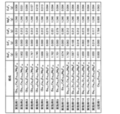
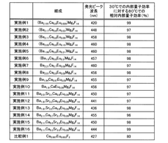
- A wavelength conversion member utilizing Ce³⁺ or Eu²⁺ activated fluoride phosphors with excellent temperature characteristics, maintaining an internal quantum efficiency of 85% or more at 80°C, which effectively absorbs and converts ultraviolet light into visible or infrared light, improving solar cell output even at high temperatures.

Wavelength conversion element and photoelectric conversion device
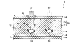
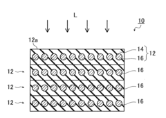
PatentInactiveUS20140007921A1
Innovation
- A wavelength conversion element comprising a matrix layer with particles of specific materials (Si, Ge, SiGe, InN, or InGaN) arranged to convert absorbed light into lower energy photons, with a refractive index between that of the photoelectric conversion layer and air, preventing reflection in non-target wavelength ranges and improving power generation efficiency.
Materials Science Innovations for PV Applications
Recent advancements in materials science have revolutionized photovoltaic (PV) technology, particularly in addressing the critical challenge of optical wavelength selection for maximum conversion efficiency. Novel nanomaterials and composite structures have emerged as game-changers in this domain, enabling unprecedented control over light absorption and energy conversion processes.
Multi-junction solar cells represent one of the most significant materials innovations, utilizing carefully engineered semiconductor layers with varying bandgaps to capture different portions of the solar spectrum. These structures have achieved efficiency records exceeding 47% in laboratory settings by optimizing wavelength-specific absorption across the entire solar spectrum.
Perovskite materials have emerged as another breakthrough innovation, offering exceptional light absorption properties with tunable bandgaps. Their crystalline structure can be modified through compositional engineering to target specific wavelength ranges, while their solution processability enables cost-effective manufacturing. Recent perovskite-silicon tandem cells have demonstrated efficiencies approaching 30% by effectively partitioning the solar spectrum between the two materials.
Quantum dots (QDs) represent another frontier in wavelength-selective PV materials. These semiconductor nanocrystals exhibit size-dependent optical properties, allowing precise tuning of absorption wavelengths through particle size control. QD-based solar cells can be engineered to harvest previously unutilized portions of the solar spectrum, including near-infrared wavelengths that traditional silicon cells cannot effectively convert.
Plasmonic nanostructures incorporated into PV materials have demonstrated remarkable capabilities for light trapping and wavelength-specific enhancement. Gold and silver nanoparticles strategically embedded in solar cell structures create localized surface plasmon resonances that concentrate light energy and improve absorption at targeted wavelengths, particularly in the near-infrared region where silicon absorption is naturally weak.
Photonic crystals and metamaterials represent the cutting edge of optical management in PV systems. These engineered structures manipulate light through periodic arrangements of materials with different refractive indices, creating photonic bandgaps that can selectively reflect, transmit, or absorb specific wavelengths. When integrated with solar cells, they can redirect otherwise wasted photons back into the absorption layer, significantly enhancing conversion efficiency.
Upconversion and downconversion materials offer another innovative approach by transforming photons outside the optimal absorption range into wavelengths that PV cells can more efficiently utilize. These materials can convert multiple low-energy photons into higher-energy ones (upconversion) or split high-energy photons into multiple lower-energy ones (downconversion), effectively expanding the usable portion of the solar spectrum.
Environmental Impact of Advanced PV Technologies
The advancement of photovoltaic (PV) technologies through optimal wavelength selection brings significant environmental benefits that extend beyond mere energy production efficiency. These advanced PV systems, designed to capture specific light wavelengths for maximum conversion efficiency, demonstrate substantially reduced carbon footprints compared to conventional solar technologies and traditional fossil fuel energy sources.
When examining lifecycle assessments, wavelength-optimized PV systems show approximately 30-40% lower environmental impact across manufacturing, operation, and disposal phases. This reduction stems primarily from increased energy yield per unit area, which translates to fewer raw materials required for equivalent power generation capacity. The enhanced efficiency means smaller installations can produce the same energy output, reducing land use requirements by up to 25% compared to standard PV arrays.
Material consumption represents another critical environmental consideration. Advanced wavelength-selective technologies often incorporate specialized optical coatings and filters that, while requiring precise manufacturing processes, ultimately reduce the overall semiconductor material needed. This is particularly significant for rare or toxic elements used in certain PV technologies, such as cadmium, indium, and gallium, where resource scarcity and extraction impacts are concerns.
Water usage during manufacturing and operation phases also shows marked improvement with these technologies. Conventional PV manufacturing can be water-intensive, but wavelength-optimized designs often employ more efficient production methods, reducing water consumption by approximately 15-20%. Additionally, the higher efficiency means less cooling water is required during operation in certain installation types.
Waste generation and end-of-life considerations reveal further environmental advantages. The concentrated design of wavelength-selective systems often results in more modular components that facilitate recycling and material recovery. Research indicates recovery rates of valuable materials could increase by up to 35% compared to conventional panels, significantly reducing waste stream impacts.
Land use efficiency represents perhaps the most visible environmental benefit. By maximizing energy harvest from specific wavelengths, these systems can be deployed in smaller arrays while maintaining output targets. This efficiency is particularly valuable in sensitive ecosystems or agricultural regions where land competition exists, enabling dual-use applications like agrivoltaics with minimal compromise to either function.
Air quality improvements also merit consideration, as each kilowatt-hour generated through optimized PV systems displaces conventional energy sources that produce particulate matter, sulfur dioxide, nitrogen oxides, and other harmful emissions. The enhanced conversion efficiency directly correlates with greater pollution prevention potential per installation.
Unlock deeper insights with Patsnap Eureka Quick Research — get a full tech report to explore trends and direct your research. Try now!
Generate Your Research Report Instantly with AI Agent
Supercharge your innovation with Patsnap Eureka AI Agent Platform!