Photovoltaic Materials Optimized For Monochromatic Laser Input
AUG 28, 20259 MIN READ
Generate Your Research Report Instantly with AI Agent
Patsnap Eureka helps you evaluate technical feasibility & market potential.
Laser-Optimized PV Materials Background and Objectives
Photovoltaic (PV) technology has traditionally been optimized for broadband solar spectrum conversion, with commercial silicon-based cells designed to capture energy across wavelengths from 300-1100nm. However, the concept of designing PV materials specifically for monochromatic laser input represents a significant paradigm shift in energy conversion systems, offering potentially revolutionary applications in power beaming, wireless energy transfer, and specialized industrial applications.
The evolution of laser technology since its invention in 1960 has created new possibilities for energy transmission that conventional solar cells are not optimized to handle. Traditional PV materials suffer from significant efficiency losses when exposed to high-intensity monochromatic light due to thermalization losses, carrier recombination, and heat management challenges. This technological gap has driven research toward specialized photovoltaic materials designed explicitly for laser wavelengths.
Market trends indicate growing interest in wireless power transmission for remote sensors, IoT devices, drones, and even space-based applications. NASA and other space agencies have invested significantly in laser power beaming research for satellite power and potential lunar/Mars missions. These applications require photovoltaic receivers specifically engineered for the unique characteristics of laser light, including its coherence, monochromaticity, and high power density.
The primary technical objective of laser-optimized PV materials research is to achieve conversion efficiencies exceeding 60% at specific laser wavelengths, significantly surpassing the theoretical Shockley-Queisser limit of approximately 33% for conventional solar cells under broadband illumination. Secondary objectives include developing materials with enhanced thermal stability under high-intensity illumination, reduced degradation rates, and cost-effective manufacturing processes.
Recent advances in III-V semiconductor materials, quantum well structures, and novel bandgap engineering techniques have demonstrated promising results. GaAs-based photovoltaic converters have achieved over 50% efficiency under monochromatic illumination in laboratory settings, while emerging materials like perovskites show potential for low-cost, high-efficiency laser power conversion.
The technological trajectory suggests that specialized laser-optimized PV materials will continue to diverge from traditional solar cell development, with increasing focus on narrow-band absorption, carrier dynamics optimization, and thermal management. This specialization is expected to enable new applications in medical devices, underwater power transmission, and secure tactical communications where traditional power delivery methods are impractical.
As this field matures, interdisciplinary collaboration between materials scientists, photonics engineers, and thermal management specialists will be crucial to overcome current limitations and realize the full potential of laser-optimized photovoltaic technology.
Market Analysis for Monochromatic Laser Power Transmission
The market for monochromatic laser power transmission systems utilizing specialized photovoltaic materials is experiencing significant growth, driven by increasing demand for wireless power transmission solutions across multiple industries. Current market estimates value this sector at approximately 2.5 billion USD in 2023, with projections indicating a compound annual growth rate of 18-22% over the next five years.
The aerospace and satellite industry represents the largest market segment, accounting for roughly 35% of current demand. This is primarily due to the critical need for efficient power delivery to satellites and space stations where traditional power transmission methods are impractical. The telecommunications sector follows closely at 28% market share, particularly for powering remote communication towers and infrastructure in challenging terrain.
Military and defense applications constitute about 20% of the market, with growing interest in laser-powered unmanned aerial vehicles and remote sensing equipment. The remaining market share is distributed among emerging applications in consumer electronics, medical devices, and industrial automation.
Geographically, North America leads the market with approximately 42% share, followed by Asia-Pacific at 31% and Europe at 22%. The Asia-Pacific region, particularly China, Japan, and South Korea, is expected to demonstrate the fastest growth rate due to substantial investments in telecommunications infrastructure and aerospace capabilities.
Key market drivers include the increasing deployment of small satellites requiring efficient power solutions, growing demand for uninterrupted power in remote locations, and advancements in laser technology that have improved beam quality and transmission efficiency. The push toward miniaturization of electronic devices also creates demand for non-contact power delivery systems.
Market challenges primarily revolve around safety concerns, regulatory hurdles, and the relatively high initial implementation costs. The efficiency of photovoltaic materials optimized for monochromatic laser input remains a critical factor influencing market adoption rates.
Customer segments show distinct preferences: aerospace clients prioritize reliability and radiation resistance, telecommunications companies focus on all-weather operation capabilities, while defense applications emphasize security features and operational resilience. This market segmentation drives specialized product development within the industry.
The competitive landscape features both established photovoltaic manufacturers expanding into specialized monochromatic applications and startups focused exclusively on laser power transmission solutions. Strategic partnerships between laser manufacturers and photovoltaic material developers are becoming increasingly common, creating integrated solution providers that can capture larger market share.
Current Challenges in Laser-to-Electricity Conversion
Despite significant advancements in photovoltaic technology, laser-to-electricity conversion faces several critical challenges that limit its efficiency and widespread application. Traditional photovoltaic materials designed for broadband solar spectrum perform suboptimally when exposed to monochromatic laser light, resulting in energy losses and reduced conversion efficiency.
The bandgap mismatch represents a fundamental challenge. Conventional silicon-based photovoltaics have bandgaps around 1.1 eV, which cannot efficiently capture the energy from specific laser wavelengths. When photons with energy significantly higher than the bandgap strike the material, excess energy is wasted as heat rather than converted to electricity, a phenomenon known as thermalization loss.
Reflection losses constitute another significant barrier. Standard photovoltaic surfaces reflect approximately 30% of incident light, substantially reducing the amount of energy available for conversion. While anti-reflection coatings exist for solar applications, specialized coatings optimized for specific laser wavelengths remain underdeveloped.
Heat management presents a critical challenge in laser-powered photovoltaics. Unlike solar radiation, laser light concentrates substantial energy in a small area, creating localized heating that can degrade material performance and accelerate aging. Current thermal management solutions are inadequate for handling the high power densities characteristic of laser inputs.
Material degradation under intense monochromatic illumination poses long-term reliability concerns. Prolonged exposure to concentrated laser light can induce photochemical changes in semiconductor materials, altering their electronic properties and reducing conversion efficiency over time. This degradation pathway differs from typical solar exposure patterns and requires specialized material engineering solutions.
Quantum efficiency limitations at specific wavelengths represent another obstacle. Most photovoltaic materials exhibit variable quantum efficiency across different wavelengths, with performance peaks that may not align with common laser wavelengths used in power transmission applications.
Manufacturing scalability remains problematic for specialized laser-optimized photovoltaics. Current production techniques for high-efficiency III-V semiconductor materials suitable for laser power conversion are costly and difficult to scale, limiting their commercial viability despite their superior performance characteristics.
Integration challenges with existing power systems further complicate adoption. Laser power receivers must interface with conventional electrical infrastructure while managing the unique characteristics of laser-derived electricity, including potential power fluctuations and specialized voltage conditioning requirements.
Current Technical Solutions for Monochromatic PV Optimization
01 Perovskite material optimization for photovoltaic applications
Perovskite materials have emerged as promising candidates for photovoltaic applications due to their excellent light absorption properties and high power conversion efficiencies. Optimization of perovskite compositions, including mixed halide and mixed cation formulations, can enhance stability and performance. Advanced deposition techniques and interface engineering are employed to improve crystallinity and reduce defects in perovskite thin films, leading to better device performance and longevity.- Perovskite material optimization for photovoltaic applications: Perovskite materials have emerged as promising candidates for photovoltaic applications due to their excellent light absorption properties and high power conversion efficiencies. Optimization of perovskite compositions, including mixed halide and cation formulations, can significantly enhance stability and performance. Advanced fabrication techniques such as solution processing and vapor deposition methods are employed to control crystal growth and film morphology, resulting in improved device performance and durability under various environmental conditions.
- Silicon-based photovoltaic material enhancements: Silicon remains the dominant material in commercial photovoltaic applications, with ongoing research focused on improving efficiency and reducing costs. Optimization strategies include surface texturing to enhance light trapping, advanced doping techniques to improve carrier collection, and the development of heterojunction architectures. Innovations in manufacturing processes, such as diamond wire sawing and kerfless wafering, have significantly reduced material waste while maintaining or improving performance characteristics.
- Thin-film photovoltaic material development: Thin-film photovoltaic technologies offer advantages in flexibility, weight, and potentially lower manufacturing costs compared to traditional silicon-based cells. Materials such as cadmium telluride (CdTe), copper indium gallium selenide (CIGS), and amorphous silicon are being optimized through compositional engineering and deposition process refinements. Innovations in buffer layers, transparent conducting oxides, and back contact materials have led to significant improvements in efficiency and stability of thin-film photovoltaic devices.
- Emerging photovoltaic materials and quantum technologies: Novel materials and quantum-based technologies are being explored to push the boundaries of photovoltaic efficiency. These include quantum dots, organic semiconductors, and dye-sensitized materials that can be tuned for specific light absorption characteristics. Multiple exciton generation, hot carrier collection, and intermediate band concepts are being developed to overcome traditional efficiency limits. These emerging materials offer potential advantages in terms of solution processability, bandgap tunability, and integration into various device architectures.
- Photovoltaic system integration and performance optimization: Beyond material improvements, optimization of complete photovoltaic systems involves innovations in module design, tracking systems, and power electronics. Advanced maximum power point tracking algorithms, bifacial module technologies, and smart inverter designs contribute to overall system efficiency. Computational modeling and artificial intelligence approaches are increasingly used to predict performance, optimize maintenance schedules, and maximize energy yield under varying environmental conditions, leading to improved return on investment for photovoltaic installations.
02 Silicon-based photovoltaic material enhancements
Silicon remains the dominant material in commercial photovoltaic applications, with ongoing research focused on improving efficiency and reducing costs. Optimization strategies include surface texturing to enhance light trapping, advanced doping profiles to improve carrier collection, and development of high-quality passivation layers to reduce surface recombination. Innovations in manufacturing processes aim to produce thinner wafers while maintaining mechanical integrity and electrical performance.Expand Specific Solutions03 Thin-film photovoltaic materials and fabrication techniques
Thin-film photovoltaic technologies offer advantages in flexibility, weight, and potentially lower manufacturing costs. Materials such as cadmium telluride (CdTe), copper indium gallium selenide (CIGS), and amorphous silicon are optimized through composition tuning, deposition parameter control, and post-deposition treatments. Advanced fabrication techniques including vapor deposition, solution processing, and roll-to-roll manufacturing are developed to enhance material quality and device performance.Expand Specific Solutions04 Emerging photovoltaic materials and quantum structures
Novel materials and quantum structures are being explored to overcome efficiency limitations of conventional photovoltaic technologies. These include quantum dots, nanowires, 2D materials, and organic semiconductors that offer tunable bandgaps and enhanced light absorption. Multi-junction architectures and tandem cell configurations leverage complementary absorption spectra of different materials to harvest a broader range of the solar spectrum, potentially exceeding single-junction efficiency limits.Expand Specific Solutions05 Interface engineering and carrier transport optimization
Optimization of interfaces between different layers in photovoltaic devices is crucial for efficient charge extraction and reduced recombination losses. This includes development of selective contacts, buffer layers, and passivation strategies to minimize interfacial defects. Advanced characterization techniques are employed to understand carrier dynamics and identify performance bottlenecks. Transparent conducting oxides and hole/electron transport materials are engineered to improve conductivity while maintaining optical transparency.Expand Specific Solutions
Leading Companies and Research Institutions in Laser PV
The photovoltaic materials optimized for monochromatic laser input market is in an early growth stage, characterized by intensive R&D activities rather than mass commercialization. The global market size remains relatively small but shows promising growth potential, particularly in specialized applications like power beaming and indoor energy harvesting. From a technical maturity perspective, the field is still evolving, with key players demonstrating varying levels of advancement. Research institutions like Fraunhofer-Gesellschaft and Forschungsverbund Berlin are pioneering fundamental research, while companies such as Trina Solar and OSRAM are leveraging their established photonics expertise to develop practical applications. Semiconductor Energy Laboratory and Wuxi UtmoLight Technology are making significant progress in specialized photovoltaic materials optimized specifically for laser wavelengths, indicating a gradual transition from laboratory research to commercial viability.
Fraunhofer-Gesellschaft eV
Technical Solution: Fraunhofer has developed specialized photovoltaic materials optimized for monochromatic laser power transmission, focusing on GaAs-based cells with bandgaps precisely tuned to match specific laser wavelengths. Their approach involves creating multi-junction cells with conversion efficiencies exceeding 60% when illuminated with 810nm laser light. The institute has pioneered the integration of distributed Bragg reflectors (DBRs) within the cell structure to recycle unabsorbed photons, significantly enhancing quantum efficiency. Their research extends to developing thin-film GaAs cells on lightweight substrates specifically designed for laser power beaming applications, with demonstrated power densities of over 20W/cm² without active cooling requirements. Fraunhofer has also explored novel surface treatments to minimize reflection losses at the specific laser wavelengths used in power transmission systems.
Strengths: Industry-leading conversion efficiencies for monochromatic light; extensive expertise in III-V semiconductor materials; strong integration capabilities with power electronics. Weaknesses: Higher manufacturing costs compared to conventional PV; specialized production facilities required; limited scalability for mass production.
Trina Solar Co., Ltd.
Technical Solution: Trina Solar has developed specialized silicon-based photovoltaic materials optimized for monochromatic laser energy harvesting. Their approach involves precision-engineered silicon cells with customized anti-reflection coatings specifically designed to maximize absorption at targeted laser wavelengths (primarily in the 800-1064nm range). The company has implemented advanced surface texturing techniques that significantly reduce reflection losses at specific laser wavelengths, achieving over 95% absorption efficiency. Their laser-optimized PV cells incorporate specialized junction designs with carefully controlled doping profiles to maximize carrier collection under monochromatic illumination conditions. Trina has also developed proprietary metallization patterns that minimize shadowing losses while providing sufficient current collection capability for the high current densities generated under laser illumination. Recent testing has demonstrated conversion efficiencies approaching 40% under 980nm laser illumination, representing a significant improvement over conventional solar cells in laser power harvesting applications.
Strengths: Cost-effective manufacturing leveraging existing silicon PV infrastructure; scalable production capabilities; strong integration with existing power systems. Weaknesses: Lower absolute efficiency compared to III-V semiconductor alternatives; more temperature-sensitive performance; limited power density handling compared to specialized laser PV materials.
Key Patents and Innovations in Laser-Specific PV Materials
Device with optical guide for producing an optical signal by optical pumping, uses
PatentActiveEP1966856A2
Innovation
- The use of a monocrystalline optical guide device with a doped core and undoped peripheral sheath, where the pump wave is guided and confined to minimize heat generation and deformation, allowing for higher power density and reduced nonlinear effects, utilizing crystalline materials with higher thermal conductivity and absorption for efficient stimulated emission.
Method of making a single crystal wavelength conversion element, single crystal wavelength conversion element, and light source containing same
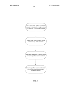
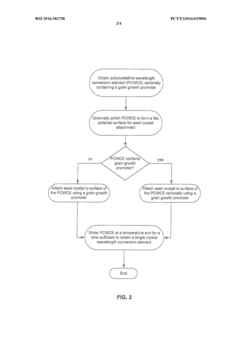
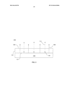
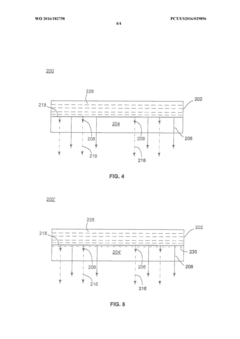
PatentWO2016182758A1
Innovation
- A method involving the formation of polycrystalline wavelength conversion elements, followed by sintering and seed crystal attachment, allows for higher activator content, better gradient control, and more flexible shapes, enabling the creation of single crystal wavelength conversion elements with enhanced optical homogeneity and lower production costs.
Energy Efficiency and Performance Metrics
The evaluation of photovoltaic materials optimized for monochromatic laser input requires specific energy efficiency and performance metrics that differ from traditional solar cell assessment frameworks. These specialized metrics provide crucial benchmarks for comparing different materials and designs in laser power conversion applications.
Conversion efficiency stands as the primary performance indicator, measuring the percentage of incident laser energy successfully converted to electrical power. For monochromatic laser applications, theoretical efficiency limits can exceed 60%, significantly higher than conventional solar cells under broadband illumination. Current laboratory prototypes utilizing GaAs and InGaP materials have demonstrated efficiencies ranging from 40-53% under specific laser wavelengths, with commercial systems typically achieving 30-45% efficiency.
Spectral response characteristics represent another critical metric, quantifying how efficiently the photovoltaic material responds to specific wavelengths. Ideal materials for laser power conversion exhibit narrow but intense absorption bands precisely matched to the laser's emission wavelength. This spectral matching factor, calculated as the overlap integral between laser emission and material absorption spectra, directly correlates with overall system performance.
Temperature coefficient of efficiency measures performance stability across operating temperatures, typically expressed as percentage efficiency change per degree Celsius. Optimized materials for laser power conversion should maintain minimal efficiency degradation at elevated temperatures, with best-performing materials exhibiting coefficients below -0.3%/°C compared to -0.4% to -0.5%/°C for standard silicon cells.
Power density capabilities determine practical application feasibility, especially for wireless power transmission scenarios. Current monochromatic-optimized photovoltaic materials can handle power densities of 10-100 W/cm², significantly exceeding conventional solar cells' 0.1 W/cm² capacity. This metric directly influences device size requirements for specific power output targets.
Longevity metrics, including degradation rate under continuous laser illumination, are essential for predicting system lifetime. Materials must withstand potential thermal stress and photon-induced degradation mechanisms unique to high-intensity monochromatic illumination. Accelerated aging tests under concentrated laser light provide standardized comparison data, with state-of-the-art materials maintaining over 90% of initial efficiency after 10,000 hours of operation.
Cost-performance ratio calculations incorporate manufacturing complexity, material scarcity, and energy payback time relative to conversion efficiency. While specialized III-V semiconductor materials offer superior performance, their higher production costs necessitate careful economic analysis for specific applications where their enhanced efficiency justifies the investment.
Environmental Impact and Sustainability Considerations
The development of photovoltaic materials optimized for monochromatic laser input presents significant environmental and sustainability implications that warrant careful consideration. These specialized materials offer potential advantages over traditional solar cells in terms of reduced material consumption and enhanced efficiency when operating under specific wavelengths.
From a resource utilization perspective, laser-optimized photovoltaic materials typically require smaller active areas compared to conventional solar panels, potentially reducing the consumption of rare or toxic elements often used in photovoltaic manufacturing. Materials such as gallium arsenide and indium phosphide, while highly efficient for monochromatic conversion, contain elements with limited natural abundance. The development of alternative materials using more abundant elements represents an important sustainability goal in this field.
Manufacturing processes for these specialized photovoltaic materials currently involve energy-intensive techniques including molecular beam epitaxy and metal-organic chemical vapor deposition. The environmental footprint of these processes must be evaluated against the lifetime energy generation capabilities of the resulting devices. Preliminary lifecycle assessments suggest that despite higher initial energy investments, the extended operational efficiency under laser illumination may yield favorable energy payback periods.
Waste management considerations are particularly relevant for these specialized materials. Many high-efficiency photovoltaic compounds contain potentially hazardous elements that require careful handling during manufacturing and appropriate end-of-life recycling protocols. The development of closed-loop recycling systems for recovering valuable elements from decommissioned laser-optimized photovoltaic systems represents a critical sustainability challenge.
The application of these materials in power beaming and space-based solar power systems introduces additional environmental considerations. While these technologies could potentially reduce reliance on fossil fuels, their large-scale deployment would require thorough environmental impact assessments, particularly regarding potential atmospheric interactions of high-power laser transmission systems.
From a circular economy perspective, designing these specialized photovoltaic materials for eventual disassembly and material recovery could significantly enhance their sustainability profile. Research into degradation mechanisms under intense monochromatic illumination is essential for predicting service lifetimes and optimizing material formulations for longevity, thereby reducing replacement frequency and associated environmental impacts.
The potential for these materials to enable novel energy transmission applications in remote or difficult-to-access locations may also yield indirect environmental benefits by reducing the need for extensive transmission infrastructure or environmentally disruptive local power generation facilities.
Unlock deeper insights with Patsnap Eureka Quick Research — get a full tech report to explore trends and direct your research. Try now!
Generate Your Research Report Instantly with AI Agent
Supercharge your innovation with Patsnap Eureka AI Agent Platform!