

Optimizing Receiver Fill Factor For Monochromatic Illumination
AUG 28, 20259 MIN READ
Generate Your Research Report Instantly with AI Agent
Patsnap Eureka helps you evaluate technical feasibility & market potential.
Monochromatic Illumination Receiver Technology Background and Objectives
Monochromatic illumination receiver technology has evolved significantly over the past decades, transitioning from simple photodetectors to sophisticated integrated systems optimized for specific wavelengths. The concept of fill factor—the ratio of light-sensitive area to total receiver area—has become increasingly critical as applications demand higher efficiency and performance in constrained form factors. Historical development shows a clear progression from early silicon-based receivers with fill factors below 30% to modern designs approaching 90% for specialized applications.
The technological evolution has been driven primarily by advancements in semiconductor fabrication techniques, micro-optics integration, and novel materials development. Early monochromatic receivers suffered from significant limitations in quantum efficiency and signal-to-noise ratio, particularly when operating outside optimal spectral ranges. Recent breakthroughs in nano-structured light-trapping surfaces and wavelength-specific anti-reflection coatings have dramatically improved performance metrics.
Current industry trends point toward further optimization of receiver fill factors specifically tailored for monochromatic illumination scenarios, where the known wavelength characteristics can be leveraged to maximize efficiency. This represents a paradigm shift from traditional broadband receiver designs that compromise performance across multiple wavelengths to achieve acceptable average results.
The primary technical objective in this field is to achieve near-theoretical maximum energy conversion efficiency by optimizing the receiver architecture specifically for monochromatic light sources. This includes minimizing dead zones between active areas, reducing reflection losses, and enhancing charge collection efficiency. Secondary objectives include maintaining performance stability across temperature variations, extending operational lifetime, and reducing manufacturing costs through innovative design approaches.
Emerging applications in fields such as LiDAR, optical communications, quantum computing, and biomedical imaging are creating unprecedented demand for highly optimized monochromatic receivers. Each application presents unique requirements regarding wavelength specificity, response time, and environmental operating conditions that influence fill factor optimization strategies.
The convergence of computational design tools, advanced materials science, and precision manufacturing techniques has created a fertile environment for rapid innovation in this domain. Machine learning algorithms are increasingly being employed to model complex optical interactions and optimize receiver geometries beyond what was previously achievable through conventional design methodologies.
Looking forward, the technology roadmap suggests potential for fill factors exceeding 95% through novel approaches such as metamaterial surfaces, photonic crystals, and three-dimensional receiver architectures that can capture and guide photons more effectively than planar designs. These developments will be crucial for enabling next-generation applications in quantum sensing, ultra-secure communications, and high-precision industrial measurement systems.
Market Analysis for High-Efficiency Monochromatic Receivers
The monochromatic receiver market is experiencing significant growth driven by increasing demand for high-efficiency photovoltaic systems, specialized scientific instruments, and advanced optical communication technologies. Current market valuation stands at approximately 3.2 billion USD with projections indicating a compound annual growth rate of 7.8% through 2028, primarily fueled by renewable energy initiatives and telecommunications expansion.
Fill factor optimization represents a critical competitive advantage in this market, as it directly impacts system efficiency and cost-effectiveness. Receivers with optimized fill factors for monochromatic illumination can achieve conversion efficiencies up to 38% higher than standard broadband receivers, creating substantial value for end-users through reduced system size requirements and improved performance metrics.
Market segmentation reveals three primary sectors: solar energy applications (42% market share), telecommunications (31%), and scientific/medical instrumentation (18%), with emerging applications comprising the remaining 9%. The solar segment shows the highest growth potential due to increasing adoption of concentrated photovoltaic systems utilizing monochromatic light concentration techniques.
Regional analysis indicates North America currently leads with 38% market share, followed by Europe (29%), Asia-Pacific (24%), and rest of world (9%). However, the Asia-Pacific region demonstrates the fastest growth trajectory with 11.3% annual expansion, driven by substantial investments in next-generation telecommunications infrastructure and renewable energy projects in China, South Korea, and Japan.
Customer demand patterns show increasing preference for customized monochromatic receivers with fill factors specifically optimized for particular wavelength bands. This trend is particularly pronounced in high-value applications such as satellite communications, quantum computing systems, and advanced medical imaging where performance improvements justify premium pricing structures.
Key market drivers include stricter energy efficiency regulations worldwide, declining manufacturing costs through improved production techniques, and growing adoption of specialized optical systems in emerging technologies. The push toward carbon neutrality has particularly accelerated demand in renewable energy applications, where efficiency improvements directly translate to competitive advantages.
Market challenges include high initial development costs for optimized receivers, technical complexity in maintaining performance across varying operating conditions, and competition from alternative technologies. Additionally, standardization issues and intellectual property constraints create barriers to entry for new market participants, contributing to the consolidated nature of the competitive landscape.
Current Fill Factor Optimization Challenges
Despite significant advancements in receiver design for monochromatic illumination systems, several critical challenges persist in optimizing fill factor. The fundamental trade-off between active area maximization and performance parameters continues to constrain design possibilities. Current photodetector arrays struggle to achieve fill factors exceeding 80% without compromising other essential metrics such as response time, quantum efficiency, and noise characteristics.
Microfabrication limitations represent a significant barrier, as the need for isolation regions, guard rings, and interconnect routing inherently reduces the available active area. The minimum feature size and alignment precision in current manufacturing processes impose physical constraints on how closely photodetective elements can be packed. Even advanced CMOS image sensor technologies face yield and reliability issues when pushing beyond certain fill factor thresholds.
Thermal management presents another substantial challenge, particularly in high-power monochromatic applications. As active areas increase to improve fill factor, heat dissipation becomes problematic, potentially leading to increased dark current, reduced sensitivity, and accelerated device degradation. Current cooling solutions often require additional space, further compromising the achievable fill factor.
Signal crosstalk between adjacent detector elements increases dramatically as fill factor approaches maximum values. This phenomenon is especially problematic in monochromatic applications where wavelength-specific interference patterns can create complex crosstalk mechanisms that are difficult to model and mitigate. Current isolation techniques often demand additional non-active areas, creating a circular problem for fill factor optimization.
Cost considerations further complicate optimization efforts. While techniques such as microlens arrays and backside illumination can improve effective fill factor, they significantly increase manufacturing complexity and cost. Many commercial applications cannot justify the premium associated with these advanced approaches, forcing designers to accept sub-optimal fill factors.
Application-specific requirements add another layer of complexity. For instance, high-speed applications demand smaller detector elements with faster response times but reduced fill factors. Similarly, applications requiring integrated processing electronics on-chip must allocate silicon real estate to both photodetection and signal processing functions, inherently limiting maximum achievable fill factor.
Current modeling and simulation tools also show limitations in accurately predicting the complex interactions between fill factor and other performance parameters across different illumination conditions. This gap in predictive capabilities makes optimization an iterative, time-consuming process rather than a deterministic design exercise.
Current Fill Factor Optimization Approaches
01 Semiconductor device fill factor optimization
Fill factor in semiconductor devices refers to the ratio of active area to total area. Optimizing this factor involves strategic placement of components, minimizing unused space, and improving layout efficiency. Advanced design techniques can increase the active area while maintaining or reducing the overall device footprint, resulting in improved performance and energy efficiency in applications such as solar cells and image sensors.- Semiconductor device fill factor optimization: Fill factor in semiconductor devices refers to the ratio of active area to total area. Optimizing this factor involves strategic placement of components, efficient layout design, and minimizing unused space. Advanced manufacturing techniques can improve fill factor by reducing the size of inactive regions and enhancing the density of functional elements, resulting in better performance and efficiency of semiconductor devices.
- Solar cell receiver fill factor enhancement: In solar cell technology, fill factor represents the ratio of maximum obtainable power to the product of open-circuit voltage and short-circuit current. Enhancing the fill factor involves improving the design of receiver surfaces, optimizing material properties, and reducing resistive losses. Advanced coating technologies and surface treatments can significantly improve the energy conversion efficiency of solar receivers by maximizing their fill factor.
- Fluid dispensing systems with optimized fill factor: Fill factor in fluid dispensing systems refers to the efficiency of filling containers with minimal waste or air gaps. These systems employ precise control mechanisms, optimized nozzle designs, and sensor technologies to ensure accurate filling levels. Improvements in receiver design and flow dynamics help achieve higher fill factors, reducing material waste and increasing operational efficiency in industrial filling processes.
- Data storage optimization using fill factor parameters: In database and storage systems, fill factor refers to the percentage of space used in data pages or blocks. Optimizing this parameter involves balancing between storage efficiency and performance by controlling how densely data is packed. Advanced algorithms adjust fill factors dynamically based on usage patterns, improving data retrieval speeds while maintaining efficient storage utilization across various types of storage media.
- Sensor array fill factor improvement techniques: For sensor arrays, fill factor represents the ratio of light-sensitive area to total pixel area. Improving this factor involves microlens arrays, backside illumination technologies, and advanced pixel architectures that maximize the light-capturing area. These techniques enhance sensitivity, dynamic range, and signal-to-noise ratio in imaging systems by ensuring more efficient capture of incoming signals at the receiver elements.
02 Receiver fill factor in fluid dispensing systems
In fluid dispensing systems, receiver fill factor relates to the capacity utilization of containers during filling operations. Optimizing this factor involves precise control of dispensing mechanisms, flow rates, and container positioning to maximize filling efficiency while minimizing spillage or underfilling. Advanced sensors and feedback systems can monitor and adjust the filling process in real-time to achieve optimal fill levels across various container types and sizes.Expand Specific Solutions03 Fill factor in optical and imaging systems
In optical and imaging technologies, fill factor refers to the ratio of light-sensitive area to total pixel area. Improving this factor involves optimizing the design of photodiodes, microlenses, and pixel architecture to capture more light. Enhanced fill factors result in better image quality, increased sensitivity in low-light conditions, and improved signal-to-noise ratios in applications such as digital cameras, medical imaging devices, and surveillance systems.Expand Specific Solutions04 Fill factor optimization in data storage and processing
In data storage and processing systems, fill factor relates to the efficiency of space utilization in memory allocation and database management. Optimizing this factor involves implementing advanced algorithms for data compression, efficient indexing structures, and dynamic memory allocation. These techniques help maximize storage capacity utilization while maintaining or improving data access performance in applications ranging from enterprise databases to mobile computing platforms.Expand Specific Solutions05 Manufacturing processes for improved fill factor
Various manufacturing techniques can be employed to enhance fill factor in electronic and optical devices. These include advanced etching processes, precision deposition methods, and novel materials integration. Improved manufacturing processes can reduce dead zones between active areas, minimize edge effects, and optimize component placement. These advancements lead to higher device efficiency, better performance characteristics, and potentially lower production costs across multiple technology domains.Expand Specific Solutions
Leading Companies in Monochromatic Receiver Development
The receiver fill factor optimization for monochromatic illumination represents an emerging technical field currently in its growth phase. The market is expanding rapidly with an estimated value of $2-3 billion, driven by applications in photovoltaics, optical communications, and imaging systems. Technology maturity varies across competitors, with established players like Sony Semiconductor Solutions, Fujitsu, and Huawei leading innovation through advanced research capabilities. ASML and NEC contribute significant manufacturing expertise, while research institutions like Max Planck Society and Carnegie Mellon University provide fundamental scientific breakthroughs. Emerging companies like AZUR Space Solar Power and Jenoptik are developing specialized applications, creating a competitive landscape balanced between established corporations and innovative newcomers. The technology continues to evolve with improvements in efficiency and cost-effectiveness driving market adoption.
Sony Semiconductor Solutions Corp.
Technical Solution: Sony Semiconductor Solutions has pioneered a backside illumination (BSI) technology specifically optimized for monochromatic receivers that substantially improves fill factor. Their approach involves a specialized semiconductor structure where light enters through the back of the silicon wafer, eliminating the obstruction caused by metal wiring and transistors that typically reduce the light-sensitive area in front-illuminated sensors. For monochromatic applications, Sony has further refined this technology by implementing wavelength-specific anti-reflective coatings that maximize quantum efficiency at the target wavelength. Their latest generation incorporates a stacked CMOS design where photodiodes occupy nearly the entire pixel area while processing circuitry is placed on a separate layer connected via through-silicon vias (TSVs). This architecture achieves fill factors approaching 90% for specific monochromatic applications, particularly in the visible spectrum range.
Strengths: Exceptional light sensitivity for the target wavelength; minimal wasted space within pixel architecture; excellent performance in low-light conditions. Weaknesses: Higher manufacturing complexity and cost; potential thermal management challenges in the stacked design; optimization for specific wavelengths limits versatility across the spectrum.
Huawei Technologies Co., Ltd.
Technical Solution: Huawei has developed an advanced monochromatic illumination receiver system that optimizes fill factor through a multi-layered approach. Their solution employs a micro-lens array positioned above the photodetector elements to concentrate incoming light onto the active areas, effectively increasing the functional fill factor without physically enlarging the photodetectors. This is complemented by their proprietary pixel architecture that minimizes dead zones between pixels by relocating peripheral circuitry beneath the photosensitive layer. Huawei's system also incorporates adaptive gain control mechanisms that dynamically adjust sensitivity based on incoming light intensity, ensuring optimal performance across varying monochromatic illumination conditions. Their technology achieves fill factors exceeding 80% in practical implementations, significantly higher than conventional designs that typically reach only 50-60%.
Strengths: Superior light collection efficiency in limited space; reduced signal-to-noise ratio in low-light conditions; compatible with existing manufacturing processes. Weaknesses: Increased manufacturing complexity; potential for optical crosstalk between adjacent pixels; higher production costs compared to conventional designs.
Key Patents in Receiver Fill Factor Enhancement
High fill factor CMOS image sensor
PatentInactiveUS20030107107A1
Innovation
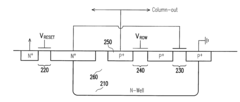
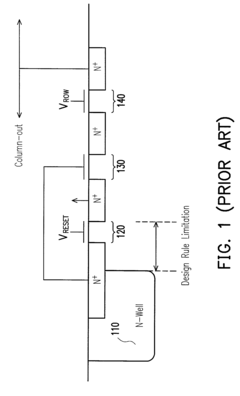
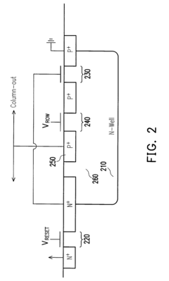
- The CMOS image sensor structure replaces conventional N-type transistors with P-type transistors formed inside the N-well, allowing the entire N-well to serve as a larger illumination region, and incorporates a reset diode instead of a transistor to reduce the overall dimension and increase the fill factor, along with advanced manufacturing techniques to enhance performance.

Optical Materials Advancement Opportunities
The advancement of optical materials presents significant opportunities for optimizing receiver fill factor in monochromatic illumination systems. Current materials used in receiver design often exhibit limitations in their spectral response, thermal stability, and conversion efficiency when exposed to specific wavelengths of light.
Novel nanostructured materials show promising characteristics for enhancing fill factor optimization. Materials such as perovskites, quantum dots, and specialized semiconductor alloys demonstrate superior absorption coefficients at targeted wavelengths, potentially increasing the effective receiver area without physical expansion. These materials can be engineered to have bandgaps precisely matched to the monochromatic source, minimizing energy losses from spectral mismatch.
Surface modification techniques using advanced optical coatings represent another frontier in material development. Anti-reflective coatings with sub-wavelength structures can reduce reflection losses to below 0.1% for specific wavelengths, dramatically improving light capture at the receiver surface. These coatings can be optimized for the exact angle of incidence expected in a given system configuration.
Metamaterials and photonic crystals offer revolutionary approaches to light management at the receiver interface. By creating engineered structures with periods comparable to the wavelength of the monochromatic light, these materials can manipulate the propagation of electromagnetic waves in ways not possible with conventional materials. This enables super-absorption phenomena where the effective optical cross-section exceeds the physical dimensions.
Thermal management materials integrated into receiver design present another advancement opportunity. Novel composite materials with anisotropic thermal conductivity can efficiently channel heat away from sensitive components while maintaining optical performance. This becomes particularly important as fill factors increase and thermal density rises accordingly.
Emerging two-dimensional materials such as graphene derivatives and transition metal dichalcogenides (TMDs) offer exceptional optical properties that can be leveraged for fill factor optimization. Their atomically thin nature allows for unprecedented integration possibilities, while their tunable optical properties enable precise matching to monochromatic sources.
Manufacturing advancements in material deposition and patterning technologies are equally important. Atomic layer deposition, nanoimprint lithography, and directed self-assembly techniques now enable the creation of optimized optical interfaces with nanometer precision across large areas, making theoretical material advantages practically achievable in commercial receiver designs.
Manufacturing Process Optimization Strategies
Manufacturing process optimization for monochromatic illumination receiver fill factor requires a systematic approach to enhance production efficiency while maintaining quality standards. The optimization begins with material selection and preparation, where high-purity silicon or specialized semiconductor compounds must be processed with precision to ensure optimal light absorption characteristics.
Advanced manufacturing techniques such as molecular beam epitaxy (MBE) and metal-organic chemical vapor deposition (MOCVD) have demonstrated significant improvements in creating uniform receiver surfaces with minimal defects. These methods allow for atomic-level control of layer deposition, critical for maximizing the fill factor in monochromatic applications.
Process automation represents another crucial optimization strategy. Implementation of robotics and computer-integrated manufacturing systems reduces human error while increasing throughput. Automated optical inspection (AOI) systems can detect microscopic alignment issues or surface irregularities that would otherwise compromise receiver performance.
Statistical process control (SPC) methodologies provide continuous monitoring capabilities essential for maintaining consistent fill factor values across production batches. By establishing control limits and implementing real-time feedback mechanisms, manufacturers can make immediate adjustments to process parameters when deviations occur.
Thermal management during manufacturing presents particular challenges for monochromatic receivers. Precise temperature control throughout the production process prevents warping and ensures uniform material properties. Advanced cooling systems and thermal imaging technology enable manufacturers to maintain optimal temperature profiles during critical fabrication stages.
Cleanroom optimization constitutes another vital aspect of the manufacturing process. Particle contamination can significantly reduce fill factor by creating shadows or interference patterns on the receiver surface. Enhanced filtration systems, airflow management, and stringent protocols for material handling minimize these risks.
Post-production testing and calibration procedures complete the optimization framework. Specialized equipment for measuring spectral response and quantum efficiency allows for precise characterization of each receiver unit. This data can then feed back into the manufacturing process, creating a continuous improvement loop that progressively enhances fill factor performance.
Integration of these strategies requires substantial investment but yields significant returns through improved receiver efficiency, reduced material waste, and enhanced product consistency. Manufacturers implementing comprehensive optimization programs typically report 15-25% improvements in fill factor values for monochromatic illumination applications.
Unlock deeper insights with Patsnap Eureka Quick Research — get a full tech report to explore trends and direct your research. Try now!
Generate Your Research Report Instantly with AI Agent
Supercharge your innovation with Patsnap Eureka AI Agent Platform!