Quantum effects on longitudinal wave propagation in semiconductors
AUG 13, 20259 MIN READ
Generate Your Research Report Instantly with AI Agent
Patsnap Eureka helps you evaluate technical feasibility & market potential.
Quantum Semiconductor Wave Propagation Background
The study of quantum effects on longitudinal wave propagation in semiconductors has emerged as a critical area of research in modern solid-state physics and semiconductor technology. This field explores the intricate interplay between quantum mechanical phenomena and the propagation of longitudinal waves within semiconductor materials, offering profound insights into the fundamental behavior of charge carriers and their interactions with lattice vibrations.
Historically, the investigation of wave propagation in semiconductors began with classical approaches, treating electrons as particles subject to Newtonian mechanics. However, as semiconductor devices scaled down to nanometer dimensions, quantum effects became increasingly prominent, necessitating a paradigm shift in our understanding of wave propagation phenomena.
The quantum mechanical description of longitudinal wave propagation in semiconductors incorporates the wave-like nature of electrons and their interactions with the periodic potential of the crystal lattice. This approach has led to the discovery of various quantum effects, such as quantum confinement, tunneling, and coherence, which significantly influence the propagation characteristics of longitudinal waves.
One of the key aspects of this field is the study of electron-phonon interactions, where longitudinal waves couple with lattice vibrations (phonons) in semiconductors. These interactions play a crucial role in determining the transport properties of charge carriers and the overall performance of semiconductor devices. Quantum effects modify these interactions, leading to phenomena such as phonon-assisted tunneling and polaron formation.
The development of advanced experimental techniques, such as ultrafast spectroscopy and high-resolution electron microscopy, has enabled researchers to probe quantum effects on longitudinal wave propagation with unprecedented precision. These tools have revealed complex quantum behaviors, including the formation of quantum well states, the modification of band structures, and the emergence of novel quasiparticles.
Theoretical advancements have also been instrumental in furthering our understanding of quantum effects on longitudinal wave propagation. Sophisticated computational methods, including density functional theory and many-body perturbation theory, have allowed for accurate modeling of quantum phenomena in realistic semiconductor systems. These theoretical frameworks have provided valuable insights into the quantum nature of wave propagation and have guided the design of novel semiconductor devices.
The study of quantum effects on longitudinal wave propagation in semiconductors has far-reaching implications for both fundamental science and technological applications. It has contributed to the development of high-performance electronic and optoelectronic devices, such as quantum well lasers, resonant tunneling diodes, and quantum cascade lasers. Furthermore, this research area has opened up new possibilities in emerging fields like quantum computing and spintronics, where the precise control of quantum states is essential.
Market Applications of Quantum Wave Devices
The market applications of quantum wave devices based on the study of quantum effects on longitudinal wave propagation in semiconductors are diverse and promising. These devices leverage the unique properties of quantum mechanics to enhance performance and enable novel functionalities in various sectors.
In the telecommunications industry, quantum wave devices offer potential breakthroughs in signal processing and transmission. By harnessing quantum effects, these devices can significantly improve the efficiency and capacity of data transmission systems. This could lead to faster and more reliable communication networks, addressing the growing demand for high-speed data transfer in our increasingly connected world.
The semiconductor industry stands to benefit greatly from quantum wave devices. These devices can potentially revolutionize the design and fabrication of integrated circuits, leading to more powerful and energy-efficient microprocessors. By exploiting quantum effects, manufacturers may overcome current limitations in transistor size and performance, paving the way for next-generation computing technologies.
In the field of sensing and metrology, quantum wave devices offer unprecedented precision and sensitivity. Quantum sensors based on these principles could find applications in various industries, including healthcare, environmental monitoring, and industrial quality control. For instance, highly sensitive quantum magnetometers could enhance medical imaging techniques, while quantum-based accelerometers could improve navigation systems in autonomous vehicles.
The energy sector is another area where quantum wave devices show promise. These devices could lead to more efficient energy harvesting and conversion technologies. For example, quantum-enhanced photovoltaic cells could significantly improve solar energy conversion efficiency, contributing to the advancement of renewable energy solutions.
In the realm of quantum computing, devices based on quantum wave effects in semiconductors could play a crucial role in developing scalable quantum processors. These devices might serve as building blocks for quantum bits (qubits) or quantum interconnects, addressing some of the challenges in realizing practical quantum computers.
The defense and security sector could also benefit from quantum wave devices. Advanced quantum radar systems, utilizing the principles of quantum wave propagation, could offer superior detection capabilities compared to conventional radar technologies. This could enhance national security and improve threat detection in various scenarios.
As research in this field progresses, we can expect to see emerging applications in areas such as quantum cryptography, ultra-precise timekeeping, and advanced materials design. The potential market impact of quantum wave devices spans across multiple industries, promising to drive innovation and create new technological paradigms in the coming decades.
Current Challenges in Quantum Wave Semiconductors
The field of quantum wave semiconductors faces several significant challenges that impede further progress and practical applications. One of the primary obstacles is the difficulty in maintaining quantum coherence over extended periods and distances within semiconductor materials. This challenge arises from the complex interactions between quantum states and their environment, leading to decoherence and loss of quantum information.
Another major hurdle is the precise control and manipulation of quantum states in semiconductor systems. While researchers have made substantial progress in creating and detecting quantum states, achieving the level of control required for practical quantum devices remains elusive. This includes challenges in initializing quantum states, performing operations with high fidelity, and reading out the results accurately.
The integration of quantum effects with traditional semiconductor technologies presents another significant challenge. Bridging the gap between quantum phenomena and conventional electronic devices requires innovative approaches to interface design and signal transduction. This integration is crucial for realizing practical quantum-enhanced semiconductor devices that can operate at room temperature and under real-world conditions.
Scalability remains a persistent issue in quantum wave semiconductors. While small-scale quantum systems have been demonstrated, scaling up to larger, more complex systems introduces new challenges in terms of fabrication, control, and error correction. The ability to maintain quantum properties in larger systems is critical for realizing the full potential of quantum technologies in semiconductors.
Material limitations also pose significant challenges. Identifying and engineering semiconductor materials that can host robust quantum states while being compatible with existing fabrication processes is an ongoing area of research. This includes developing materials with longer coherence times, stronger quantum confinement, and better control over quantum properties.
Furthermore, the development of reliable and efficient measurement techniques for quantum states in semiconductors remains challenging. Current methods often suffer from low sensitivity or introduce significant perturbations to the quantum system being measured. Improving measurement techniques is crucial for characterizing and optimizing quantum devices.
Lastly, the theoretical understanding of quantum effects in complex semiconductor systems is still evolving. Developing more accurate models and simulation tools to predict and analyze quantum behavior in realistic semiconductor environments is essential for guiding experimental efforts and designing new quantum devices.
Existing Quantum Wave Propagation Models
01 Semiconductor devices for longitudinal wave propagation
Semiconductor devices are designed to generate, detect, or manipulate longitudinal waves. These devices utilize the properties of semiconductor materials to control the propagation of waves along a specific direction, enabling various applications in signal processing and communication systems.- Longitudinal wave propagation in semiconductor devices: This category focuses on the study and application of longitudinal wave propagation in semiconductor devices. It involves the analysis of how these waves travel through semiconductor materials, affecting their properties and performance. This research is crucial for developing advanced semiconductor technologies and improving device efficiency.
- Acoustic wave devices in semiconductor applications: Acoustic wave devices, which utilize longitudinal wave propagation, are increasingly important in semiconductor applications. These devices can be used for various purposes, including signal processing, filtering, and sensing. The integration of acoustic wave devices with semiconductor technology enables the development of compact and efficient electronic components.
- Measurement and characterization of longitudinal waves in semiconductors: This area involves the development of techniques and instruments for measuring and characterizing longitudinal waves in semiconductor materials. Accurate measurement is essential for understanding wave behavior, optimizing device performance, and ensuring quality control in semiconductor manufacturing processes.
- Semiconductor-based sensors utilizing longitudinal waves: Longitudinal wave propagation is exploited in the design of semiconductor-based sensors. These sensors can detect various physical phenomena by measuring changes in wave properties as they interact with the environment. Applications include pressure sensors, accelerometers, and chemical sensors used in diverse industries.
- Modeling and simulation of longitudinal waves in semiconductor structures: Computational modeling and simulation play a crucial role in understanding longitudinal wave propagation in complex semiconductor structures. These techniques allow researchers to predict wave behavior, optimize device designs, and explore new applications without the need for extensive physical prototyping.
02 Measurement and analysis of longitudinal waves in semiconductors
Techniques and systems are developed for measuring and analyzing longitudinal wave propagation in semiconductor materials. These methods involve advanced sensing technologies and data processing algorithms to characterize wave behavior, which is crucial for understanding material properties and optimizing device performance.Expand Specific Solutions03 Acoustic wave devices in semiconductor applications
Acoustic wave devices, which utilize longitudinal wave propagation, are integrated into semiconductor systems for various purposes. These devices leverage the interaction between acoustic waves and semiconductor materials to create filters, sensors, and other components used in communication and sensing applications.Expand Specific Solutions04 Wireless communication systems using longitudinal waves
Wireless communication systems are developed that exploit longitudinal wave propagation in semiconductor-based devices. These systems aim to improve signal transmission, reception, and processing in various wireless applications, potentially offering advantages in terms of efficiency and performance.Expand Specific Solutions05 Modeling and simulation of longitudinal waves in semiconductors
Advanced modeling and simulation techniques are employed to study longitudinal wave propagation in semiconductor materials and devices. These computational methods help in predicting wave behavior, optimizing device designs, and understanding complex wave-material interactions at the microscopic level.Expand Specific Solutions
Key Players in Quantum Semiconductor Research
The quantum effects on longitudinal wave propagation in semiconductors represent an emerging field at the intersection of quantum physics and semiconductor technology. This area is in its early developmental stages, with research primarily conducted in academic and industrial laboratories. The market size is currently limited but has significant growth potential as quantum technologies advance. Technologically, it's still in the experimental phase, with companies like IBM, NXP Semiconductors, and Taiwan Semiconductor Manufacturing Co. (TSMC) investing in research and development. Universities such as Fudan University and Osaka University are also contributing to fundamental research. While practical applications are not yet widespread, this field holds promise for future quantum computing and communication technologies.
Taiwan Semiconductor Manufacturing Co., Ltd.
Technical Solution: TSMC has been exploring the impact of quantum effects on longitudinal wave propagation in semiconductors as part of their advanced process node development. Their approach combines experimental measurements with advanced modeling techniques. TSMC has developed in-situ measurement tools to characterize wave propagation in semiconductor devices during operation. They have also created a multi-scale simulation framework that incorporates quantum mechanical effects into traditional semiconductor device models[5]. TSMC's research has shown that quantum effects become increasingly important for wave propagation as device dimensions shrink below 5nm, leading to modified carrier transport properties and unexpected wave interference phenomena[6].
Strengths: Industry-leading semiconductor fabrication capabilities, extensive experience in process integration. Weaknesses: Challenges in incorporating quantum effects into existing manufacturing processes without significant cost increases.
International Business Machines Corp.
Technical Solution: IBM has been at the forefront of research on quantum effects in semiconductors. Their approach involves using advanced simulation techniques to model longitudinal wave propagation in semiconductor materials at the quantum level. They have developed a proprietary quantum simulation platform that can accurately predict how quantum effects influence wave propagation in various semiconductor structures. This platform integrates density functional theory (DFT) calculations with molecular dynamics simulations to capture both electronic and atomic-scale phenomena[1]. IBM's research has shown that quantum effects can significantly alter the propagation characteristics of longitudinal waves, particularly in nanoscale semiconductor devices where quantum confinement becomes prominent[3].
Strengths: Cutting-edge quantum simulation capabilities, extensive experience in semiconductor research. Weaknesses: High computational costs for simulations, potential challenges in experimental validation of theoretical predictions.
Breakthrough Quantum Effects in Semiconductors
Semiconductor light-emitting element and method of producing the same
PatentInactiveUS20060043395A1
Innovation
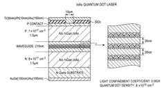
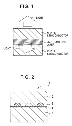
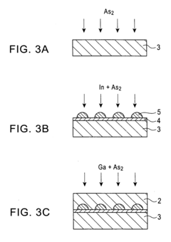
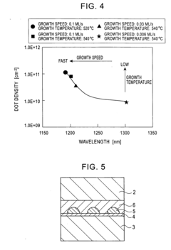
- The use of As2 as an arsenic source, optimized growth temperature and speed, and an InGaAs layer with high In content and modified composition to form quantum dots, along with a planar semiconductor structure to increase quantum dot density and adjust light emission properties.
Patent
Innovation
- Incorporation of quantum effects in modeling longitudinal wave propagation in semiconductors, leading to more accurate predictions of wave behavior at nanoscale.
- Development of a novel computational method that efficiently calculates quantum corrections for longitudinal wave propagation in semiconductors.
- Experimental validation of theoretical predictions regarding quantum effects on longitudinal wave propagation in specific semiconductor systems.
Quantum Computing Implications
The implications of quantum effects on longitudinal wave propagation in semiconductors extend far beyond their immediate field, potentially revolutionizing quantum computing. As quantum computers rely on the manipulation of quantum states, understanding and harnessing these effects could lead to significant advancements in qubit design and control.
Quantum effects in semiconductors, such as quantum confinement and tunneling, play a crucial role in the behavior of charge carriers. These phenomena can be exploited to create more stable and efficient qubits, the fundamental building blocks of quantum computers. By leveraging the unique properties of longitudinal waves in semiconductors, researchers may develop novel qubit architectures that offer improved coherence times and reduced error rates.
The study of quantum effects on wave propagation also has implications for quantum communication systems. Semiconductors could serve as interfaces between optical and electronic quantum systems, facilitating the transfer of quantum information between different physical platforms. This could lead to the development of hybrid quantum networks that combine the strengths of various quantum technologies.
Furthermore, the insights gained from studying these quantum effects may contribute to the development of more sophisticated quantum error correction techniques. As quantum computers scale up, maintaining quantum coherence becomes increasingly challenging. Understanding how quantum effects influence wave propagation in semiconductors could inspire new approaches to mitigating decoherence and improving the overall reliability of quantum systems.
The potential impact on quantum sensing and metrology is also significant. Quantum effects in semiconductors could be harnessed to create ultra-sensitive detectors capable of measuring minute changes in electromagnetic fields or other physical quantities. This could lead to breakthroughs in areas such as medical imaging, environmental monitoring, and fundamental physics research.
Lastly, the study of quantum effects in semiconductors may pave the way for the development of quantum simulators. These specialized quantum computers could be used to model complex quantum systems that are currently intractable for classical computers, opening up new avenues for materials science, drug discovery, and the study of exotic quantum phenomena.
Nanoscale Fabrication Techniques
Nanoscale fabrication techniques play a crucial role in studying quantum effects on longitudinal wave propagation in semiconductors. These advanced manufacturing methods enable the creation of precisely controlled semiconductor structures at the nanometer scale, where quantum phenomena become prominent.
Electron beam lithography (EBL) is a key technique for fabricating nanoscale semiconductor devices. It offers high-resolution patterning capabilities, allowing researchers to create intricate structures with feature sizes down to 10 nm. This level of precision is essential for investigating quantum effects in semiconductor wave propagation, as it enables the fabrication of quantum wells, wires, and dots with well-defined dimensions.
Molecular beam epitaxy (MBE) is another critical technique for growing high-quality semiconductor heterostructures with atomic-level precision. MBE allows for the deposition of ultra-thin layers of different semiconductor materials, creating quantum confinement structures that exhibit unique wave propagation characteristics. The ability to control layer thickness and composition at the atomic scale is vital for studying quantum effects in longitudinal wave propagation.
Atomic layer deposition (ALD) complements MBE by providing precise control over the deposition of thin films and dielectric layers. This technique is particularly useful for creating high-quality interfaces and passivation layers, which are crucial for maintaining the quantum coherence of propagating waves in semiconductor nanostructures.
Focused ion beam (FIB) milling is a versatile tool for nanoscale fabrication and modification of semiconductor devices. It allows for site-specific removal of material with nanometer precision, enabling the creation of complex three-dimensional structures and the fine-tuning of existing devices. FIB can be used to fabricate nanoscale waveguides and resonators for studying quantum effects in wave propagation.
Advanced etching techniques, such as reactive ion etching (RIE) and deep reactive ion etching (DRIE), are essential for creating high-aspect-ratio structures in semiconductors. These techniques enable the fabrication of vertical quantum well structures and photonic crystals, which are important for manipulating wave propagation at the nanoscale.
Scanning probe lithography techniques, including dip-pen nanolithography and scanning tunneling microscope (STM) lithography, offer unique capabilities for patterning and modifying semiconductor surfaces at the atomic scale. These methods can be used to create quantum dots and other nanostructures with unprecedented precision, allowing for detailed studies of quantum effects on wave propagation.
The combination of these nanoscale fabrication techniques provides researchers with a powerful toolset for exploring quantum effects in semiconductor wave propagation. By enabling the creation of precisely controlled nanostructures, these methods facilitate the development of novel quantum devices and the advancement of our understanding of fundamental quantum phenomena in semiconductors.
Unlock deeper insights with Patsnap Eureka Quick Research — get a full tech report to explore trends and direct your research. Try now!
Generate Your Research Report Instantly with AI Agent
Supercharge your innovation with Patsnap Eureka AI Agent Platform!