

Quantum Tunneling Influence on Device Scalability: Analysis
SEP 4, 20259 MIN READ
Generate Your Research Report Instantly with AI Agent
PatSnap Eureka helps you evaluate technical feasibility & market potential.
Quantum Tunneling Background and Scalability Goals
Quantum tunneling represents a fundamental quantum mechanical phenomenon where particles penetrate through potential energy barriers that would be insurmountable according to classical physics. This effect emerges from the wave-particle duality principle, allowing electrons to "tunnel" through thin insulating layers in semiconductor devices. First observed in the early 20th century, quantum tunneling has evolved from a theoretical curiosity to a critical consideration in modern semiconductor engineering, particularly as device dimensions approach the nanometer scale.
The historical progression of semiconductor technology has been characterized by continuous miniaturization following Moore's Law, which predicted the doubling of transistor density approximately every two years. However, as device dimensions have shrunk below 10nm, quantum effects including tunneling have transitioned from negligible phenomena to dominant factors limiting further scaling. This paradigm shift necessitates a comprehensive understanding of tunneling mechanisms to establish realistic scaling goals.
Current semiconductor roadmaps identify quantum tunneling as one of the primary physical barriers to continued device miniaturization. Gate oxide tunneling, source-to-drain tunneling, and band-to-band tunneling all increase exponentially as dimensions decrease, resulting in higher leakage currents, increased power consumption, and degraded device performance. These effects become particularly pronounced when gate oxide thicknesses fall below 2nm or channel lengths below 5nm.
The technical objectives for addressing quantum tunneling challenges encompass several dimensions. Short-term goals focus on mitigating tunneling effects through material engineering, including high-k dielectrics and strain engineering. Medium-term objectives involve architectural innovations such as multi-gate structures, vertical transistors, and tunnel FETs that can leverage tunneling effects constructively. Long-term aspirations include developing "tunneling-immune" technologies or paradigms that operate fundamentally differently from conventional CMOS.
Industry consensus suggests that quantum tunneling will ultimately necessitate a departure from traditional scaling approaches. The International Roadmap for Devices and Systems (IRDS) projects that beyond the 3nm node, revolutionary rather than evolutionary approaches will be required. This includes potential shifts toward quantum computing, neuromorphic architectures, or other emerging computing paradigms where tunneling might be harnessed rather than suppressed.
The technical trajectory indicates that future scalability goals must balance physical limitations with practical engineering solutions, recognizing that quantum tunneling represents both a challenge to overcome and potentially a phenomenon to exploit in next-generation computing architectures.
Market Demand for Nanoscale Device Technologies
The market for nanoscale device technologies has experienced exponential growth over the past decade, primarily driven by the semiconductor industry's relentless pursuit of Moore's Law. As conventional CMOS technology approaches its physical limits, quantum tunneling effects have transitioned from being merely theoretical concerns to critical practical limitations affecting device performance and reliability. This shift has created a substantial market demand for innovative solutions that can address quantum tunneling challenges while enabling further miniaturization.
Current market analysis indicates that the semiconductor industry continues to invest heavily in research and development of sub-10nm technologies, with annual R&D expenditures exceeding $60 billion globally. The demand for smaller, more energy-efficient devices remains strong across multiple sectors, including consumer electronics, telecommunications, automotive, and emerging fields such as Internet of Things (IoT) and artificial intelligence (AI) applications.
The smartphone market, representing one of the largest consumers of advanced semiconductor technologies, continues to drive demand for more powerful yet energy-efficient processors. This has created a significant market pull for solutions that can mitigate quantum tunneling effects while maintaining performance improvements. Industry forecasts suggest that the market for tunneling-resistant gate materials and novel transistor architectures will grow at a compound annual growth rate of 14.3% through 2028.
Enterprise data centers and cloud computing infrastructure providers represent another major market segment demanding advanced nanoscale technologies. With data processing requirements doubling approximately every two years, these customers require chips that deliver higher performance per watt, directly driving interest in quantum tunneling mitigation technologies. Market research indicates that data center operators are willing to pay premium prices for processors that can deliver even marginal improvements in energy efficiency.
The automotive sector has emerged as a rapidly growing market for advanced semiconductor technologies, particularly with the acceleration of electric vehicle adoption and autonomous driving capabilities. These applications require highly reliable, energy-efficient computing platforms that can operate in challenging environmental conditions, creating specific demands for tunneling-resistant device technologies.
Medical device manufacturers and healthcare technology companies are also increasingly investing in miniaturized electronics for implantable and wearable devices. This sector places particular emphasis on ultra-low power consumption and long-term reliability, making quantum tunneling mitigation a critical consideration in their technology roadmaps.
Market analysis reveals that customers across these diverse sectors are increasingly aware of quantum tunneling challenges and are actively seeking solutions that can extend device scalability beyond current limitations. This awareness has translated into concrete procurement specifications and willingness to invest in next-generation technologies that address these fundamental physical constraints.
Current Challenges in Quantum Tunneling Mitigation
Quantum tunneling presents significant challenges for semiconductor device scaling as dimensions approach sub-10nm nodes. The primary obstacle lies in electron leakage through potential barriers that classical physics would deem impenetrable. This quantum mechanical phenomenon becomes increasingly pronounced as gate oxide thicknesses decrease, leading to substantial off-state leakage currents that compromise device performance and power efficiency.
Current mitigation strategies face fundamental limitations. High-k dielectric materials, while effective at reducing direct tunneling, introduce interface quality issues that degrade carrier mobility. The trade-off between equivalent oxide thickness and leakage current creates a scaling bottleneck that traditional CMOS technology struggles to overcome. Additionally, the variability in tunneling rates due to atomic-scale fluctuations in barrier thickness presents significant manufacturing challenges for consistent device performance.
Band engineering approaches, such as strained silicon and SiGe channels, offer partial solutions by modifying the effective mass of carriers, but these techniques reach diminishing returns below 5nm. The industry faces a critical challenge in balancing quantum confinement effects, which can beneficially increase the effective bandgap, against the detrimental increase in tunneling probability as dimensions shrink.
Gate-all-around architectures and nanowire transistors represent promising structural innovations to improve electrostatic control, but they introduce complex three-dimensional tunneling paths that are difficult to model and control. The multi-directional nature of tunneling in these advanced structures requires sophisticated simulation tools that can accurately capture quantum effects in three dimensions.
Temperature dependence adds another layer of complexity, as tunneling exhibits less temperature sensitivity than thermionic emission, making it increasingly dominant at lower operating temperatures. This creates challenges for cryogenic computing applications where traditional leakage reduction techniques become less effective.
Power constraints present perhaps the most immediate practical challenge. As tunneling-induced leakage increases exponentially with scaling, static power consumption threatens to exceed thermal design limits for high-performance computing applications. The industry's push toward higher integration densities exacerbates this issue, creating a fundamental conflict between performance scaling and power efficiency.
Material interface engineering remains an active research area, with efforts focused on creating atomically precise barriers to minimize trap-assisted tunneling. However, achieving consistent atomic-level precision in high-volume manufacturing environments presents significant yield and reliability challenges that have yet to be fully resolved.
Current Approaches to Quantum Tunneling Management
01 Nanoscale quantum tunneling device architectures
Quantum tunneling devices can be scaled down to nanometer dimensions through innovative architectures that maintain functionality at reduced sizes. These approaches include using novel materials and structures that preserve quantum effects at smaller scales, enabling higher integration density while managing quantum confinement effects. Advanced fabrication techniques allow for precise control of tunnel barrier thickness and composition, which is critical for maintaining device performance as dimensions decrease.- Nanoscale quantum tunneling device architectures: Quantum tunneling devices can be scaled down to nanometer dimensions through innovative architectural designs. These architectures leverage quantum mechanical effects at extremely small scales to create functional electronic components. By reducing the physical dimensions of tunneling junctions and barriers, these devices can achieve higher integration density while maintaining quantum coherence. Advanced fabrication techniques enable precise control of tunnel barrier thickness and composition, which is critical for reliable device operation at nanoscale.
- Materials engineering for scalable quantum tunneling: Novel materials play a crucial role in enhancing the scalability of quantum tunneling devices. Two-dimensional materials, compound semiconductors, and engineered heterostructures provide superior tunneling characteristics and stability at reduced dimensions. These materials enable precise control of quantum barrier properties, improving tunneling efficiency and reducing variability between devices. Temperature stability and resistance to environmental factors are also enhanced through materials selection, allowing for more robust operation in practical applications.
- Integration with conventional semiconductor technology: Successful scaling of quantum tunneling devices requires compatibility with existing semiconductor manufacturing processes. Integration approaches that combine quantum tunneling elements with CMOS technology enable hybrid systems that leverage the advantages of both paradigms. Techniques for interfacing quantum tunneling components with traditional electronic circuits address signal conversion, amplification, and noise reduction challenges. This integration pathway provides a practical route to incorporating quantum tunneling functionality into commercial electronic systems.
- Quantum tunneling for memory and computing applications: Quantum tunneling mechanisms can be harnessed for next-generation memory and computing architectures with improved scalability. These devices utilize controlled electron tunneling to represent and process information, potentially offering advantages in power consumption and processing density. Resonant tunneling diodes, quantum dot arrays, and single-electron transistors demonstrate pathways to implement computational functions through quantum mechanical effects. The inherent quantum nature of these devices enables novel computing paradigms that may overcome scaling limitations of conventional transistor technology.
- Fabrication techniques for mass production: Advanced fabrication methods are essential for scaling quantum tunneling devices from laboratory demonstrations to commercial production. Techniques such as atomic layer deposition, molecular beam epitaxy, and electron beam lithography enable precise control of critical dimensions at the nanoscale. Statistical process control methods address variability challenges in tunnel barrier formation, ensuring consistent device performance across large production volumes. These manufacturing approaches focus on yield improvement, defect reduction, and cost-effective production to enable practical applications of quantum tunneling technology.
02 Multi-layer and 3D integration techniques
Three-dimensional integration and multi-layer fabrication techniques enable improved scalability of quantum tunneling devices. By stacking quantum structures vertically rather than expanding horizontally, these approaches achieve higher device density while maintaining quantum coherence. These techniques incorporate specialized interlayer connections and isolation methods to prevent interference between quantum elements while allowing for complex circuit designs in a compact form factor.Expand Specific Solutions03 Temperature and environmental stability solutions
Scalable quantum tunneling devices require solutions for temperature and environmental stability. Advanced cooling systems and thermal management techniques allow quantum effects to be maintained at higher operating temperatures, reducing the need for extreme cryogenic conditions. Materials engineering approaches create more robust tunnel barriers that are less susceptible to thermal fluctuations and environmental interference, enabling practical deployment in various applications.Expand Specific Solutions04 Semiconductor-compatible quantum tunneling fabrication
Integration of quantum tunneling devices with conventional semiconductor manufacturing processes enables large-scale production. These approaches adapt existing CMOS fabrication techniques to create quantum structures, allowing for compatibility with standard integrated circuit production lines. The use of silicon-based platforms and industry-standard lithography enables quantum tunneling devices to benefit from the scaling advantages of semiconductor manufacturing while maintaining the unique properties required for quantum effects.Expand Specific Solutions05 Error correction and signal amplification methods
As quantum tunneling devices scale to smaller dimensions, error correction and signal amplification become critical for maintaining reliable operation. Advanced error correction algorithms compensate for quantum decoherence and tunneling variations that become more pronounced at smaller scales. Novel signal amplification techniques preserve quantum information while boosting signal strength, enabling the integration of quantum tunneling devices into larger systems with conventional electronics.Expand Specific Solutions
Leading Companies in Quantum-Aware Semiconductor Design
Quantum tunneling's impact on device scalability is currently in a transitional phase, with the market expanding as semiconductor manufacturers confront physical limitations in traditional transistor designs. The global market for quantum-resistant technologies is projected to reach significant scale as devices approach sub-5nm nodes. Technologically, industry leaders like Intel, TSMC, and IBM are developing innovative solutions to mitigate tunneling effects, with Intel focusing on gate engineering, TSMC advancing 3D transistor architectures, and IBM exploring novel materials. Academic institutions including Princeton, USC, and Fudan University are contributing fundamental research, while specialized quantum companies like D-Wave Systems and IQM Finland are exploring alternative computing paradigms that leverage quantum phenomena rather than fighting against them.
Intel Corp.
Technical Solution: Intel has developed advanced gate architectures to mitigate quantum tunneling effects in sub-10nm nodes. Their FinFET technology evolved into Gate-All-Around (GAA) structures that provide better electrostatic control, reducing leakage currents caused by quantum tunneling. Intel's research includes high-k dielectric materials that increase the effective oxide thickness while maintaining capacitance, creating a more effective barrier against electron tunneling. Their process integrates strain engineering to modify the band structure of channel materials, altering tunneling probabilities. Intel has also pioneered the use of III-V semiconductor materials with higher electron mobility to compensate for performance losses due to tunneling effects. Recent developments include their PowerVia backside power delivery network that separates power delivery from the signal interconnect network, allowing for reduced operating voltages while maintaining performance targets despite quantum mechanical constraints.
Strengths: Intel's vertical integration allows for coordinated materials, process, and design solutions to quantum tunneling challenges. Their extensive manufacturing experience enables rapid implementation of theoretical advances. Weaknesses: Their solutions often require complex manufacturing processes that increase production costs and may limit yield in early implementation phases.
Taiwan Semiconductor Manufacturing Co., Ltd.
Technical Solution: TSMC has implemented a comprehensive approach to quantum tunneling mitigation in their advanced process nodes. Their N3 (3nm) technology utilizes nanosheet transistor architecture that provides superior gate control compared to FinFETs, significantly reducing off-state leakage caused by quantum tunneling. TSMC has developed specialized high-mobility channel materials and strain engineering techniques that modify the effective mass of carriers, directly impacting tunneling probabilities. Their research includes the implementation of ultra-thin body SOI (Silicon-On-Insulator) substrates that provide better confinement of carriers and reduce short-channel effects exacerbated by tunneling. TSMC's gate stack engineering incorporates atomic layer deposition techniques for creating precisely controlled high-k dielectric layers with optimized band alignment to minimize gate leakage. They've also pioneered the use of work function engineering in metal gates to tune threshold voltages without compromising the tunneling barrier properties, allowing for better performance-power tradeoffs in the quantum tunneling limited regime.
Strengths: TSMC's massive scale allows for extensive experimentation and rapid implementation of solutions across multiple technology nodes simultaneously. Their close partnerships with design houses enable co-optimization of devices and circuits to work within quantum mechanical constraints. Weaknesses: Their solutions tend to be optimized for high-performance computing applications, sometimes at the expense of power efficiency in more constrained applications.
Key Innovations in Tunneling Barrier Technologies
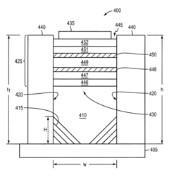
Semiconductor switching device employing a quantum dot structure
PatentActiveUS8445967B2
Innovation
- A semiconductor device employing a quantum dot structure with a semiconductor island encapsulated by dielectric material layers, where the thickness of these layers is less than 2 nm to enable quantum tunneling, allowing for low leakage current and effective switching even at low operational voltages.


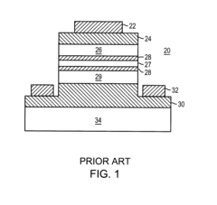
Quantum tunneling devices and circuits with lattice-mismatched semiconductor structures
PatentActiveUS7875958B2
Innovation
- The integration of III-V and II-VI materials using aspect ratio trapping (ART) epitaxial techniques and chemical vapor deposition (CVD) methods on Si substrates, allowing for the fabrication of tunneling devices with reduced defect density and improved performance, enabling the formation of high-density, low-power logic and memory circuits.
Materials Science Advancements for Tunneling Control
Recent advancements in materials science have opened new frontiers for controlling quantum tunneling effects in semiconductor devices. High-k dielectric materials, including hafnium oxide (HfO2) and zirconium oxide (ZrO2), have revolutionized gate insulation by maintaining adequate capacitance while minimizing leakage currents. These materials effectively increase the physical thickness of gate dielectrics while preserving their electrical properties, directly addressing tunneling challenges in sub-10nm nodes.
Two-dimensional materials represent another breakthrough area, with hexagonal boron nitride (h-BN) and transition metal dichalcogenides (TMDs) demonstrating exceptional tunneling barrier properties. Their atomically precise structures enable unprecedented control over electron transport, with monolayer thickness variations producing significant changes in tunneling probabilities. This precision allows for engineered tunneling barriers that can be tailored for specific device requirements.
Strain engineering has emerged as a powerful technique for modulating band structures and tunneling characteristics. By applying mechanical stress to semiconductor materials, researchers can alter the effective mass of charge carriers and modify tunneling probabilities. Silicon-germanium (SiGe) alloys with controlled strain profiles have shown particular promise in managing tunneling currents while maintaining carrier mobility.
Atomic layer deposition (ALD) techniques have transformed manufacturing capabilities, enabling the creation of ultra-thin films with atomic-level precision. This advancement allows for the development of engineered barrier structures with precisely controlled thickness gradients and composition profiles, directly influencing tunneling behavior. The ability to deposit conformal layers on complex 3D structures has been crucial for advanced device architectures.
Interface engineering has become increasingly important as devices scale down. Novel passivation techniques using hydrogen, nitrogen, and sulfur treatments have demonstrated significant reductions in interface states that contribute to unwanted tunneling. Additionally, the development of epitaxial dielectrics that form pristine interfaces with semiconductor substrates has minimized defect-assisted tunneling mechanisms.
Quantum confinement effects are being harnessed through nanoscale material engineering. Quantum dots, nanowires, and other low-dimensional structures exhibit discrete energy levels that can be designed to either enhance or suppress tunneling depending on application requirements. These structures are particularly promising for tunnel field-effect transistors (TFETs) where band-to-band tunneling is the desired operating mechanism.
Energy Efficiency Impact of Quantum Leakage
Quantum tunneling, a fundamental quantum mechanical phenomenon, significantly impacts the energy efficiency of semiconductor devices as they continue to scale down. This leakage mechanism becomes increasingly prominent when device dimensions approach the nanometer scale, creating substantial challenges for power management in modern integrated circuits.
The energy efficiency degradation due to quantum leakage manifests primarily through increased static power consumption. As transistor gate oxides become thinner to maintain electrostatic control at smaller nodes, electrons can tunnel through these barriers even when devices are nominally in their "off" state. This tunneling current contributes to standby power consumption that can account for 30-50% of total chip power in advanced technology nodes below 10nm.
Experimental measurements across multiple technology generations demonstrate an exponential increase in leakage power as gate oxide thickness decreases. For instance, the transition from 45nm to 22nm nodes showed approximately a 3x increase in gate leakage current density per unit area, directly translating to higher power density requirements and thermal management challenges.
The energy efficiency impact extends beyond individual transistors to system-level considerations. Mobile and IoT devices particularly suffer from quantum leakage effects as their battery life is directly compromised. Data centers face escalating cooling costs, with quantum tunneling contributing significantly to their total energy footprint. Current estimates suggest that leakage power due to quantum effects accounts for approximately 15-20% of global data center energy consumption.
Material innovations have attempted to address these challenges through high-k dielectric implementation, which allows for physically thicker gate insulators while maintaining equivalent electrical characteristics. However, these solutions introduce their own efficiency trade-offs, including reduced carrier mobility and increased interface trapping states that impact dynamic performance.
The energy efficiency impact also creates a fundamental limit to voltage scaling. Historically, reducing supply voltage has been a primary method for improving energy efficiency, but quantum tunneling establishes a practical lower bound. Below certain threshold voltages (approximately 0.5V in current technologies), the energy savings from voltage reduction are negated by exponentially increasing leakage currents.
Future projections indicate that without revolutionary approaches to device architecture or materials, quantum leakage will establish a practical limit to the energy efficiency improvements possible through traditional scaling. This represents a critical inflection point in semiconductor technology evolution, where alternative computing paradigms may become necessary to continue the historical trend of improved computational efficiency.
Unlock deeper insights with PatSnap Eureka Quick Research — get a full tech report to explore trends and direct your research. Try now!
Generate Your Research Report Instantly with AI Agent
Supercharge your innovation with PatSnap Eureka AI Agent Platform!