Refining X-ray Diffraction For Layered Nanostructures
FEB 27, 20269 MIN READ
Generate Your Research Report Instantly with AI Agent
PatSnap Eureka helps you evaluate technical feasibility & market potential.
X-ray Diffraction Nanostructure Analysis Background and Objectives
X-ray diffraction has emerged as a cornerstone analytical technique in materials science since its discovery in the early 20th century. The fundamental principle relies on the interaction between X-ray photons and crystalline structures, where constructive interference patterns reveal atomic arrangements according to Bragg's law. Traditional XRD techniques have proven highly effective for bulk crystalline materials, providing detailed structural information about lattice parameters, phase composition, and crystallographic orientations.
The advent of nanotechnology has introduced unprecedented challenges in structural characterization, particularly for layered nanostructures. These materials, including two-dimensional materials like graphene, transition metal dichalcogenides, and engineered multilayer systems, exhibit unique properties that differ significantly from their bulk counterparts. The reduced dimensionality and finite size effects create distinct diffraction signatures that conventional XRD approaches struggle to interpret accurately.
Current limitations in X-ray diffraction analysis of layered nanostructures stem from several fundamental issues. Peak broadening effects obscure critical structural details, while weak diffraction intensities from nanoscale volumes challenge detection sensitivity. The presence of structural defects, layer stacking disorders, and interface effects further complicate the diffraction patterns, making quantitative analysis extremely challenging.
The technological evolution toward advanced electronic devices, energy storage systems, and catalytic applications has intensified the demand for precise structural characterization of layered nanomaterials. Modern applications require atomic-level understanding of layer thickness, interlayer spacing, strain distribution, and defect concentrations. These parameters directly influence material properties and device performance, making accurate characterization essential for technological advancement.
The primary objective of refining X-ray diffraction for layered nanostructures centers on developing enhanced analytical methodologies that overcome current limitations. This involves advancing both instrumental capabilities and data analysis algorithms to extract meaningful structural information from complex diffraction patterns. The goal encompasses improving detection sensitivity for weak signals, developing robust peak deconvolution methods, and establishing reliable quantitative analysis protocols.
Secondary objectives include creating standardized measurement procedures specifically tailored for layered nanomaterials and developing predictive models that correlate diffraction signatures with material properties. The ultimate aim is to establish X-ray diffraction as a routine, reliable characterization tool for layered nanostructures, enabling rapid quality control and structural optimization in both research and industrial settings.
Market Demand for Advanced XRD Characterization Tools
The semiconductor industry represents the largest market segment driving demand for advanced XRD characterization tools specifically designed for layered nanostructures. As device dimensions continue to shrink and manufacturers increasingly adopt complex multilayer architectures, traditional XRD techniques prove insufficient for characterizing thin films, quantum wells, and heterostructures with nanometer-scale precision. Major semiconductor fabrication facilities require enhanced analytical capabilities to ensure quality control and process optimization in advanced node production.
The emerging two-dimensional materials sector has created substantial demand for specialized XRD solutions capable of analyzing graphene, transition metal dichalcogenides, and other layered materials. Research institutions and commercial developers working with these materials need precise structural characterization tools to understand interlayer spacing, stacking order, and defect structures that directly impact electronic and optical properties.
Energy storage and conversion technologies present another significant market driver. Battery manufacturers developing solid-state electrolytes and advanced electrode materials require sophisticated XRD analysis to characterize layered cathode materials, understand lithium intercalation mechanisms, and monitor structural changes during cycling. Similarly, photovoltaic cell manufacturers need advanced characterization tools for thin-film solar cells and perovskite-based devices.
The pharmaceutical and biotechnology sectors increasingly demand advanced XRD capabilities for analyzing drug delivery systems, particularly lipid nanoparticles and layered pharmaceutical compounds. These applications require precise characterization of molecular arrangements and phase transitions in complex layered structures.
Market growth is further accelerated by the expanding nanotechnology research landscape, where academic institutions and industrial research centers require sophisticated analytical tools for fundamental studies of layered nanomaterials. Government funding initiatives supporting materials science research and national competitiveness in advanced manufacturing technologies continue to drive procurement of cutting-edge characterization equipment.
The integration of artificial intelligence and machine learning capabilities into XRD systems has created additional market opportunities, as users seek automated analysis solutions that can handle the complexity of layered nanostructure data interpretation. This technological convergence addresses the growing need for high-throughput characterization in both research and production environments.
Current XRD Limitations for Layered Nanomaterial Analysis
Traditional X-ray diffraction techniques face significant challenges when applied to layered nanostructure analysis, primarily due to the fundamental limitations of conventional XRD instrumentation and methodology. The most prominent constraint lies in the insufficient angular resolution of standard diffractometers, which struggle to distinguish between closely spaced diffraction peaks characteristic of layered materials with similar d-spacings. This limitation becomes particularly pronounced when analyzing multilayer structures with periodicities in the nanometer range.
Peak broadening effects present another critical challenge, as they obscure the fine structural details essential for accurate characterization of layered nanomaterials. The inherent peak width in conventional XRD measurements often exceeds the separation between adjacent reflections from different layers, making it impossible to resolve individual layer contributions. This broadening stems from both instrumental factors and sample-related effects, including finite crystallite size and microstrain variations within the nanostructured layers.
The penetration depth limitations of standard XRD configurations create additional complications for surface-sensitive layered nanostructures. Conventional XRD typically probes several micrometers into the sample, potentially averaging signals from multiple structural regions and masking the specific characteristics of thin surface layers or interfaces. This depth averaging effect significantly reduces the technique's sensitivity to near-surface structural variations that are often critical in layered nanomaterial applications.
Texture and preferred orientation effects pose substantial analytical challenges, as layered nanostructures frequently exhibit strong crystallographic alignment that distorts intensity distributions in conventional powder diffraction patterns. Standard XRD analysis assumes random crystallite orientation, an assumption that fails dramatically for layered systems where growth processes naturally induce preferential alignment along specific crystallographic directions.
The limited dynamic range of conventional XRD detectors further constrains the analysis of layered nanostructures, where weak superlattice reflections often coexist with intense primary diffraction peaks. The inability to simultaneously measure both strong and weak reflections with adequate precision prevents comprehensive structural characterization of complex multilayer systems.
Sample preparation requirements for conventional XRD often prove incompatible with delicate layered nanostructures, as standard mounting procedures may induce mechanical stress or structural damage that alters the native layer arrangement and introduces artifacts into the diffraction data.
Current XRD Solutions for Layered Material Characterization
01 X-ray diffraction apparatus and detector systems
Advanced X-ray diffraction systems incorporate specialized detector configurations and apparatus designs to improve measurement accuracy and efficiency. These systems may include multi-dimensional detectors, optimized geometric arrangements, and enhanced signal processing capabilities. The apparatus designs focus on reducing noise, improving resolution, and enabling faster data acquisition for crystallographic analysis.- X-ray diffraction apparatus and detector systems: Advanced X-ray diffraction systems incorporate specialized detector configurations and apparatus designs to improve measurement accuracy and efficiency. These systems may include multi-dimensional detectors, optimized geometric arrangements, and enhanced signal processing capabilities. The apparatus designs focus on reducing noise, improving resolution, and enabling faster data acquisition for crystallographic analysis.
- X-ray diffraction analysis methods for material characterization: Various analytical methods utilize X-ray diffraction techniques to characterize material properties, including crystal structure, phase composition, and crystallinity. These methods involve specific measurement protocols, data processing algorithms, and interpretation techniques to extract structural information from diffraction patterns. Applications include quality control, material identification, and structural analysis of crystalline and semi-crystalline materials.
- X-ray diffraction instrumentation with improved optical components: Enhanced optical components and beam conditioning systems are employed in X-ray diffraction instruments to optimize beam characteristics and improve measurement quality. These innovations include specialized monochromators, collimators, and focusing elements that control beam intensity, wavelength selection, and spatial distribution. The improvements enable better signal-to-noise ratios and more precise diffraction measurements.
- Automated X-ray diffraction systems and data processing: Automated systems integrate hardware and software components to streamline X-ray diffraction measurements and analysis. These systems feature automated sample handling, real-time data acquisition, and computational algorithms for pattern analysis and phase identification. The automation reduces human error, increases throughput, and enables high-volume screening applications in research and industrial settings.
- Portable and compact X-ray diffraction devices: Miniaturized X-ray diffraction devices provide field-deployable and point-of-use analytical capabilities with reduced size and power requirements. These compact systems maintain analytical performance while offering portability for on-site material analysis, quality assurance, and rapid screening applications. Design innovations focus on integrating components efficiently while maintaining measurement accuracy and reliability.
02 X-ray diffraction methods for material characterization
Specific methodologies have been developed for analyzing material properties using X-ray diffraction techniques. These methods enable determination of crystal structure, phase composition, crystallinity, and orientation of various materials. The techniques can be applied to pharmaceuticals, polymers, metals, and other substances to assess their structural characteristics and quality parameters.Expand Specific Solutions03 X-ray diffraction data processing and analysis
Computational methods and algorithms have been developed to process and interpret X-ray diffraction data more effectively. These approaches include pattern recognition, peak identification, phase analysis, and quantitative determination of crystalline components. Advanced software solutions enable automated analysis and provide enhanced accuracy in structural determination from diffraction patterns.Expand Specific Solutions04 Portable and compact X-ray diffraction devices
Miniaturized X-ray diffraction instruments have been designed for field applications and point-of-use analysis. These compact systems maintain analytical capabilities while offering improved portability and ease of operation. The devices are suitable for on-site material identification, quality control, and rapid screening applications where traditional laboratory equipment is impractical.Expand Specific Solutions05 X-ray diffraction applications in pharmaceutical and chemical analysis
X-ray diffraction techniques are specifically applied to pharmaceutical formulations and chemical compounds for polymorph identification, crystallinity assessment, and quality control. These applications enable determination of solid-state forms, detection of phase transitions, and verification of drug substance identity. The methods are critical for ensuring product consistency and regulatory compliance in pharmaceutical manufacturing.Expand Specific Solutions
Key Players in XRD Equipment and Nanostructure Analysis
The X-ray diffraction refinement for layered nanostructures field represents a mature yet rapidly evolving technological landscape driven by advanced materials characterization needs. The market demonstrates substantial growth potential, particularly in semiconductor, energy storage, and advanced materials sectors. Technology maturity varies significantly across players, with established instrumentation companies like Rigaku Corp., Bruker Technologies Ltd., and Shimazu KK leading commercial solutions, while research institutions such as MIT, Fraunhofer-Gesellschaft, and Japan Synchrotron Radiation Research Institute drive fundamental innovations. Industrial giants including Samsung Electronics, TSMC, and TDK Corp. represent major end-users pushing technological boundaries. The competitive landscape spans from specialized X-ray equipment manufacturers like Sigray Inc. and Rigaku Innovative Technologies to comprehensive technology conglomerates, creating a dynamic ecosystem where academic research, commercial instrumentation, and industrial applications converge to advance nanoscale characterization capabilities.
Sigray, Inc.
Technical Solution: Sigray develops innovative X-ray analytical instruments with advanced capabilities for nanostructure characterization. Their technology features high-brightness X-ray sources, novel X-ray optics, and specialized detection systems optimized for analyzing layered nanomaterials. The company's solutions incorporate unique beam shaping technologies and advanced imaging capabilities that enable detailed structural analysis of complex nanostructured materials. Their systems provide enhanced spatial resolution and improved signal-to-noise ratios, making them particularly effective for characterizing thin films, multilayers, and other nanoengineered structures with precise layer-by-layer analysis capabilities.
Strengths: Innovative X-ray optics technology, superior spatial resolution capabilities. Weaknesses: Relatively new market presence, limited established user base.
Samsung Electronics Co., Ltd.
Technical Solution: Samsung Electronics applies X-ray diffraction techniques in their semiconductor and display manufacturing processes for quality control and characterization of layered nanostructures. Their approach focuses on integrating XRD analysis into production workflows for monitoring thin film deposition, interface quality, and structural properties of multilayer device architectures. The company utilizes advanced metrology systems that combine XRD with other analytical techniques to ensure precise control over nanostructured materials used in their electronic devices. Their technology emphasizes high-throughput analysis capabilities and automated data processing for manufacturing environment applications.
Strengths: Large-scale manufacturing integration, extensive R&D resources, proven industrial applications. Weaknesses: Technology primarily focused on internal manufacturing needs rather than general research applications.
Core XRD Innovations for Nanoscale Layer Analysis
Rapid X-ray diffraction method for structural analysis of a nano material on a surface or at an interface and for structural analysis of a solid/liquid interface, and apparatus used for the method
PatentInactiveUS20060032433A1
Innovation
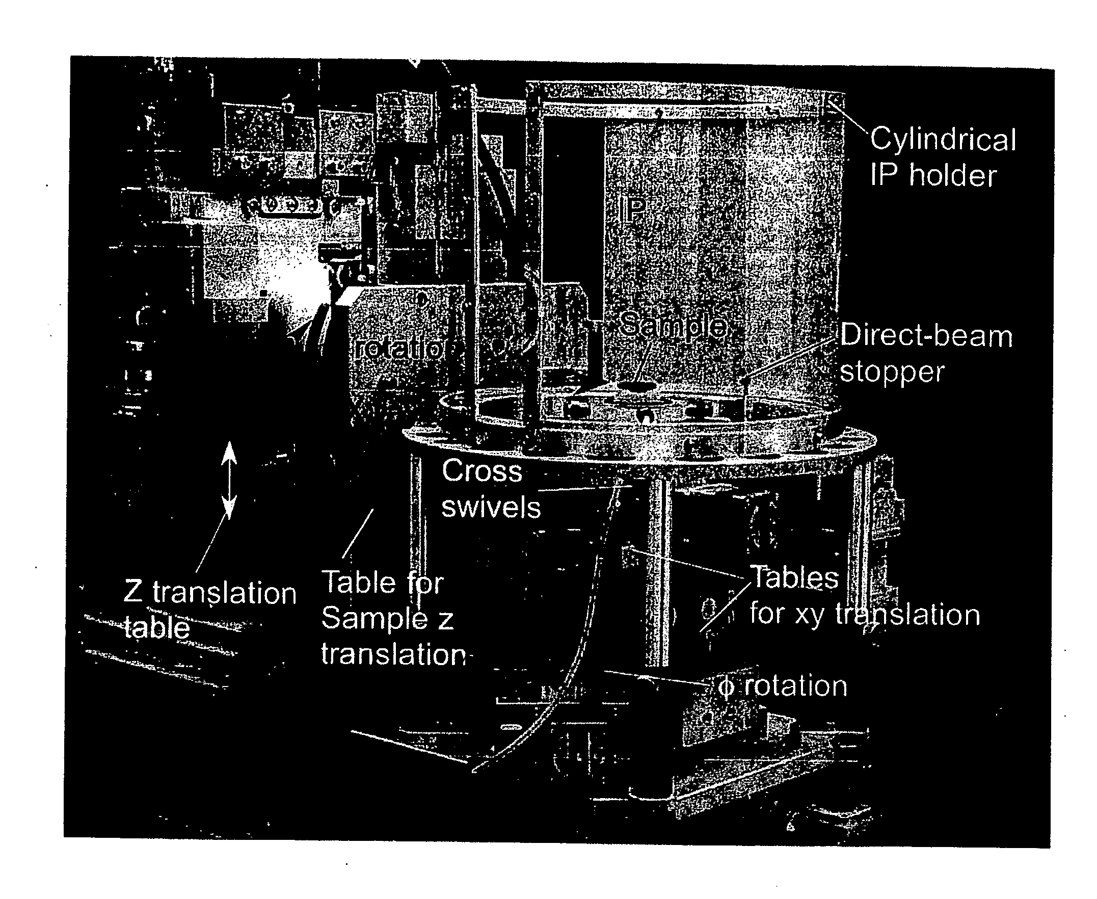
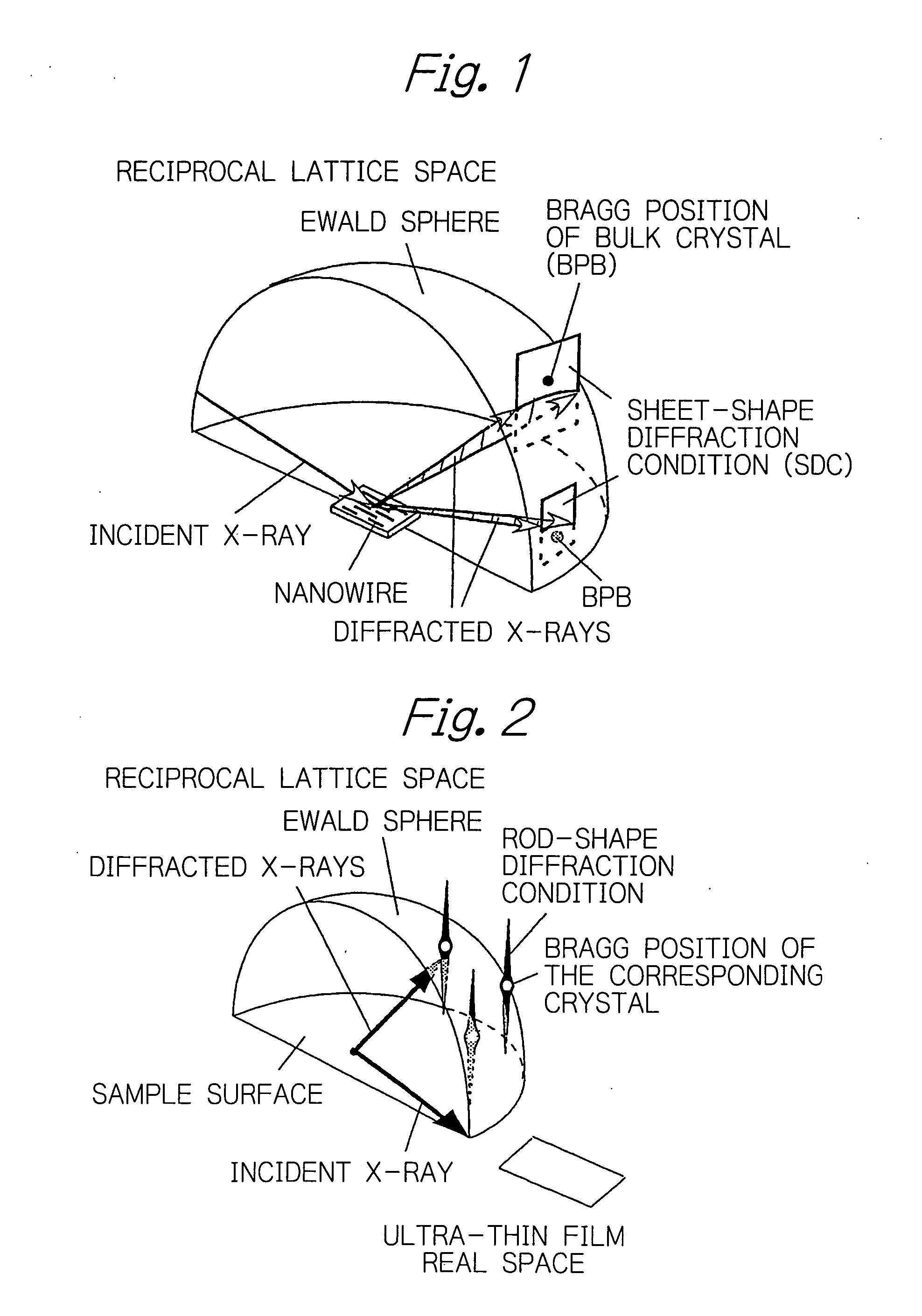
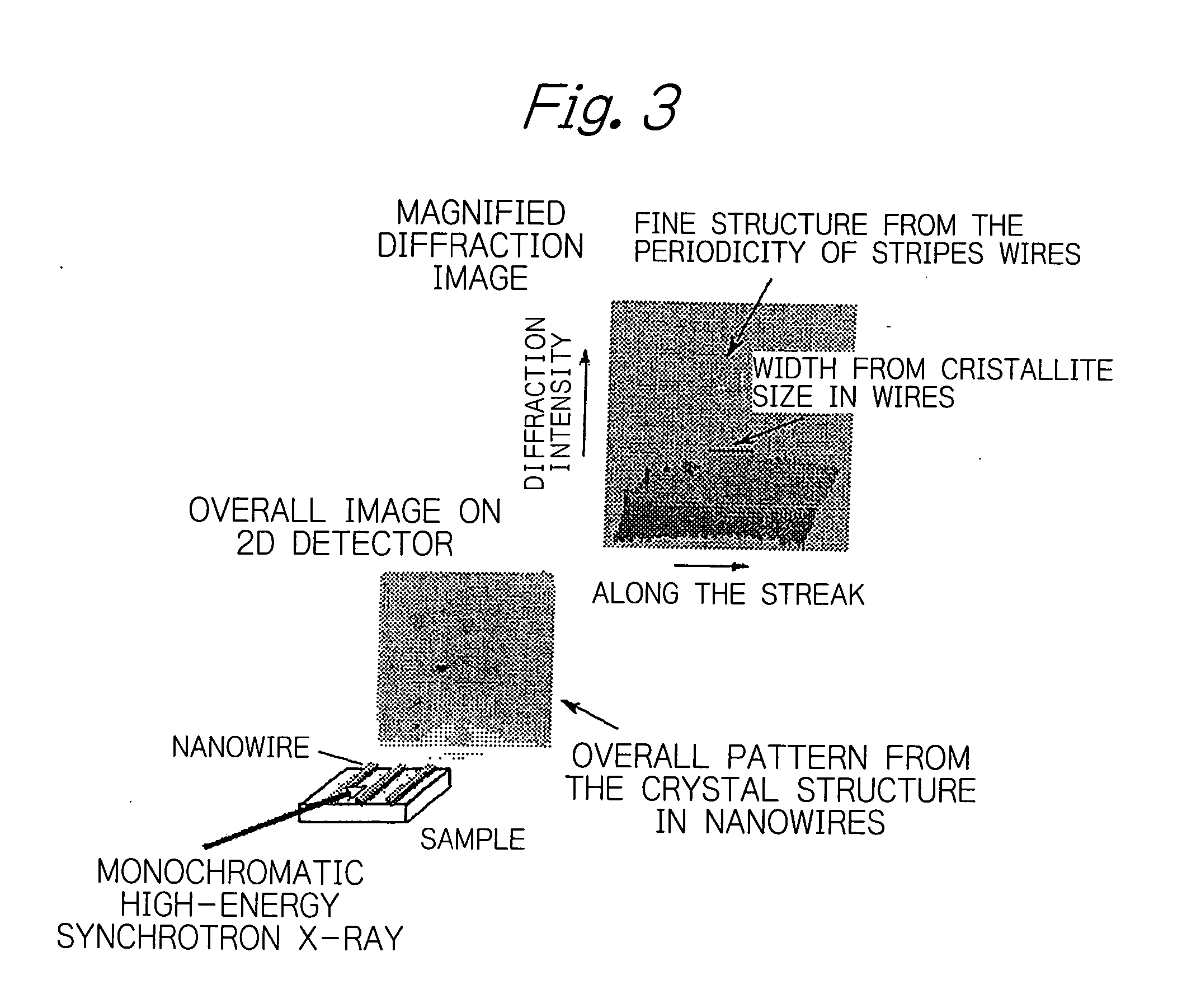
- The method employs monochromatic high-energy x-rays with wavelengths of 0.1 nanometers or shorter for a single exposure, using a two-dimensional detector to capture diffraction images without rotating the sample or detector, allowing for rapid determination of crystallographic structural information, including crystallinity, domain size, and orientation, and enabling analysis of solution/solid interfacial structures with a simple apparatus.

X-ray apparatus for analyzing three-dimensional nanostructures and method for analyzing three-dimensional nanostructures
PatentPendingUS20250334528A1
Innovation
- An X-ray apparatus and method utilizing X-rays with a wavelength greater than or equal to 0.154 nm, which collects scattered X-rays reflected by the sample to analyze structural information based on scattered intensities and angles, employing a system with an X-ray source, reflection device, and detector to focus and collect scattered X-rays for detailed nanostructure analysis.


Safety Standards for High-Energy X-ray Equipment
The development of refined X-ray diffraction techniques for layered nanostructures necessitates the implementation of comprehensive safety standards for high-energy X-ray equipment. These standards are critical as the enhanced resolution and penetration capabilities required for nanostructure analysis often demand significantly higher X-ray energies than conventional diffraction systems.
International safety frameworks, primarily established by the International Electrotechnical Commission (IEC) and the International Atomic Energy Agency (IAEA), provide foundational guidelines for high-energy X-ray equipment operation. The IEC 60601 series specifically addresses medical electrical equipment safety, while IEC 61010 covers laboratory equipment safety requirements. These standards mandate radiation shielding specifications, with lead equivalency requirements scaling proportionally to beam energy levels.
Personnel protection protocols constitute a fundamental component of safety standards, encompassing radiation monitoring, exposure limits, and training requirements. The ALARA principle (As Low As Reasonably Achievable) governs operational procedures, requiring continuous monitoring of radiation levels and implementation of administrative controls. Personal dosimetry systems must be calibrated for the specific energy ranges employed in nanostructure analysis.
Equipment design standards mandate multiple safety interlocks, emergency shutdown systems, and fail-safe mechanisms. High-energy X-ray systems require redundant safety circuits, beam containment systems, and automated exposure termination capabilities. Shielding calculations must account for both primary and scattered radiation, with particular attention to the unique scattering patterns generated by layered nanostructures.
Facility requirements include specialized room design with appropriate shielding materials, ventilation systems for ozone management, and restricted access controls. The enhanced beam intensities used in nanostructure diffraction necessitate upgraded shielding calculations and potentially thicker barrier materials compared to standard X-ray facilities.
Regular safety audits, equipment calibration protocols, and maintenance procedures ensure ongoing compliance with evolving safety standards. These requirements become increasingly stringent as beam energies approach synchrotron-level intensities, demanding specialized expertise in radiation safety management and continuous monitoring of emerging safety technologies.
Environmental Impact of Advanced XRD Manufacturing
The manufacturing of advanced X-ray diffraction equipment for layered nanostructure analysis presents significant environmental considerations that extend beyond traditional XRD systems. The precision requirements for detecting nanoscale features necessitate enhanced manufacturing processes that consume substantially more energy and resources compared to conventional diffractometers.
Advanced XRD systems require high-purity materials and ultra-precise components, leading to increased material extraction and processing demands. The production of specialized detectors, such as hybrid pixel detectors and position-sensitive detectors, involves rare earth elements and semiconductor materials that require energy-intensive purification processes. These manufacturing steps generate considerable carbon emissions and produce hazardous waste streams that require specialized treatment facilities.
The fabrication of high-resolution goniometers and sample stages demands exceptional mechanical precision, often requiring multiple machining iterations and quality control processes. This results in increased material waste and energy consumption during production. Additionally, the manufacturing of advanced X-ray sources, including rotating anodes and liquid metal jet systems, involves complex metallurgical processes that contribute to environmental burden through both energy consumption and chemical waste generation.
Packaging and transportation of these sophisticated instruments present additional environmental challenges due to their size, weight, and sensitivity requirements. Specialized protective materials and climate-controlled shipping methods increase the carbon footprint associated with global distribution networks.
However, the industry has begun implementing sustainable manufacturing practices, including closed-loop cooling systems, waste heat recovery, and recycling programs for rare materials. Some manufacturers are adopting life-cycle assessment methodologies to quantify and minimize environmental impacts throughout the production process. The development of more efficient X-ray sources and detector technologies also contributes to reduced operational energy requirements, partially offsetting manufacturing impacts over the instrument's lifetime.
Unlock deeper insights with PatSnap Eureka Quick Research — get a full tech report to explore trends and direct your research. Try now!
Generate Your Research Report Instantly with AI Agent
Supercharge your innovation with PatSnap Eureka AI Agent Platform!