X-ray Diffraction For Precise Elemental Mapping
FEB 27, 20268 MIN READ
Generate Your Research Report Instantly with AI Agent
PatSnap Eureka helps you evaluate technical feasibility & market potential.
XRD Elemental Mapping Background and Objectives
X-ray diffraction has emerged as a cornerstone analytical technique in materials science since its discovery in the early 20th century. Traditional XRD methods have primarily focused on phase identification and crystallographic structure determination through powder diffraction patterns. However, the evolution toward precise elemental mapping represents a significant advancement that bridges the gap between bulk analysis and spatially resolved characterization.
The fundamental principle underlying XRD elemental mapping relies on the unique diffraction signatures of different crystalline phases containing specific elements. When X-rays interact with crystalline materials, they produce characteristic diffraction patterns that can be correlated with elemental composition and distribution. This approach differs from conventional energy-dispersive X-ray spectroscopy by providing both compositional and structural information simultaneously.
Current technological developments have been driven by the increasing demand for nanoscale material characterization in semiconductor manufacturing, advanced ceramics, and pharmaceutical crystallography. The miniaturization of electronic devices and the complexity of modern composite materials require analytical techniques capable of resolving elemental distributions at sub-micrometer scales while maintaining crystallographic sensitivity.
The primary objective of advancing XRD elemental mapping technology centers on achieving spatial resolution comparable to electron microscopy techniques while retaining the superior penetration depth and non-destructive nature of X-ray analysis. This involves developing high-brilliance X-ray sources, advanced focusing optics, and sophisticated detector systems capable of rapid data acquisition with minimal beam damage.
Technical goals include reducing measurement times from hours to minutes, improving spatial resolution from micrometers to tens of nanometers, and enhancing detection sensitivity for trace elements within crystalline matrices. Additionally, the integration of machine learning algorithms for pattern recognition and automated phase identification represents a crucial objective for making this technology accessible to broader industrial applications.
The ultimate vision encompasses real-time elemental mapping capabilities that can monitor dynamic processes such as phase transformations, diffusion phenomena, and chemical reactions in operando conditions. This would enable unprecedented insights into material behavior under realistic operating conditions, supporting the development of next-generation materials with tailored properties and enhanced performance characteristics.
Market Demand for Precise XRD Elemental Analysis
The global market for precise X-ray diffraction elemental analysis is experiencing robust growth driven by increasing demands across multiple industrial sectors. Materials science research institutes and semiconductor manufacturers represent the largest consumer segments, requiring high-resolution elemental mapping capabilities for advanced material characterization and quality control processes. The pharmaceutical industry has emerged as another significant market driver, utilizing precise XRD analysis for polymorph identification, crystalline structure determination, and drug development validation.
Manufacturing industries, particularly in aerospace and automotive sectors, demonstrate growing adoption of precise XRD elemental mapping for failure analysis, material verification, and component quality assurance. These applications require sub-micron spatial resolution and accurate phase identification capabilities that traditional analytical methods cannot provide. The renewable energy sector, including solar panel and battery manufacturers, increasingly relies on precise elemental mapping to optimize material compositions and enhance performance characteristics.
Academic and research institutions constitute a substantial market segment, with universities and national laboratories investing in advanced XRD systems for fundamental research in crystallography, geology, and nanotechnology. Government-funded research programs focusing on advanced materials development have created sustained demand for high-precision analytical instrumentation.
Geographically, North America and Europe maintain dominant market positions due to established research infrastructure and significant industrial manufacturing bases. The Asia-Pacific region shows the highest growth potential, driven by expanding semiconductor manufacturing, increased research investments, and growing pharmaceutical industries in countries like China, Japan, and South Korea.
Market trends indicate increasing demand for automated systems with enhanced throughput capabilities, as laboratories seek to process larger sample volumes while maintaining analytical precision. Integration with complementary analytical techniques and development of portable XRD systems for field applications represent emerging market opportunities. The growing emphasis on material sustainability and recycling processes has created new application areas requiring precise elemental characterization capabilities.
Current XRD Mapping Limitations and Technical Challenges
Current X-ray diffraction mapping technologies face significant spatial resolution constraints that fundamentally limit their precision in elemental analysis. Traditional XRD systems typically achieve spatial resolutions in the range of 10-100 micrometers, which proves inadequate for modern materials characterization requirements, particularly in semiconductor devices, advanced ceramics, and nanostructured materials where feature sizes often fall below these detection limits.
The inherent beam divergence and focusing limitations of conventional X-ray optics represent a primary technical bottleneck. Standard X-ray sources produce divergent beams that require complex focusing systems, yet even with advanced Kirkpatrick-Baez mirrors or capillary optics, achieving sub-micrometer resolution remains challenging due to aberrations and intensity losses. This limitation becomes particularly pronounced when attempting to map compositional variations in thin films or multilayer structures.
Data acquisition speed presents another critical challenge, as high-resolution XRD mapping requires extensive scanning protocols that can extend measurement times to several hours or days for comprehensive area coverage. The trade-off between spatial resolution, measurement time, and signal-to-noise ratio creates operational constraints that limit practical applications in industrial settings where rapid characterization is essential.
Sample preparation and positioning accuracy introduce additional complications, particularly for irregular or curved surfaces where maintaining consistent X-ray incidence angles becomes problematic. Environmental factors such as thermal drift, mechanical vibrations, and beam stability further compromise measurement precision, especially during extended mapping sessions required for high-resolution analysis.
Detection sensitivity limitations become apparent when analyzing light elements or trace constituents, where weak diffraction signals may be obscured by background noise or overlapping peaks from major phases. This challenge is compounded in heterogeneous materials where phase identification requires discrimination between closely related crystal structures.
The computational burden associated with processing large datasets from high-resolution XRD mapping creates workflow bottlenecks. Phase identification algorithms often struggle with complex diffraction patterns from multiphase materials, requiring significant manual intervention and expert interpretation that limits automation potential and introduces subjective bias in results analysis.
Current XRD Solutions for Elemental Mapping
01 X-ray diffraction imaging systems with detector arrays
Advanced X-ray diffraction systems utilize specialized detector arrays to capture diffraction patterns for elemental mapping. These systems employ multi-pixel detectors that can simultaneously collect diffraction data from multiple points on a sample, enabling rapid spatial mapping of elemental composition. The detector configurations are optimized for energy-dispersive or wavelength-dispersive analysis, allowing for high-resolution elemental distribution mapping across sample surfaces.- X-ray diffraction imaging systems with detector arrays: Advanced X-ray diffraction systems utilize specialized detector arrays to capture diffraction patterns for elemental mapping. These systems employ multi-pixel detectors that can simultaneously collect diffraction data from multiple points on a sample, enabling rapid spatial mapping of elemental composition. The detector configurations are optimized for energy-dispersive or wavelength-dispersive analysis, allowing for high-resolution elemental distribution mapping across sample surfaces.
- Scanning and positioning mechanisms for spatial mapping: Precise scanning mechanisms are employed to systematically move either the X-ray beam or the sample to acquire diffraction data from multiple locations. These systems incorporate motorized stages, beam steering optics, and position encoding systems that enable automated raster scanning or targeted area analysis. The positioning accuracy directly impacts the spatial resolution of the resulting elemental maps, with some systems achieving sub-micrometer precision for detailed microstructural analysis.
- Data processing and image reconstruction algorithms: Sophisticated computational methods are used to process raw diffraction data and reconstruct elemental distribution maps. These algorithms perform background subtraction, peak identification, phase analysis, and quantitative elemental determination from diffraction patterns. Advanced processing techniques include machine learning approaches for pattern recognition, real-time data analysis during acquisition, and three-dimensional reconstruction from multiple projection angles to create volumetric elemental maps.
- Combined X-ray fluorescence and diffraction analysis: Integrated analytical systems combine X-ray diffraction with X-ray fluorescence spectroscopy to provide complementary elemental and crystallographic information. These hybrid instruments can simultaneously or sequentially perform both measurements, correlating elemental composition with crystal structure and phase distribution. The combined approach enhances analytical capabilities by providing both chemical identification and structural characterization in a single mapping experiment.
- Micro-beam and nano-beam X-ray diffraction techniques: Focused X-ray beam technologies enable high spatial resolution elemental mapping at microscopic and nanoscopic scales. These techniques utilize specialized X-ray optics such as capillary lenses, zone plates, or multilayer mirrors to concentrate X-ray radiation into beams with diameters ranging from micrometers to nanometers. The focused beams allow for detailed mapping of elemental distribution in heterogeneous materials, grain structures, and interfaces with exceptional spatial resolution.
02 Combined X-ray fluorescence and diffraction analysis
Integration of X-ray fluorescence spectroscopy with diffraction techniques enables simultaneous elemental identification and crystallographic analysis. This combined approach allows for comprehensive material characterization by correlating elemental composition with crystal structure information. The methodology provides both qualitative and quantitative elemental mapping while preserving spatial resolution, making it particularly useful for heterogeneous samples and multi-phase materials.Expand Specific Solutions03 Scanning and positioning systems for spatial mapping
Precision scanning mechanisms and sample positioning systems enable systematic collection of diffraction data across sample areas to generate elemental maps. These systems incorporate motorized stages, beam scanning optics, and coordinate control systems that allow for automated raster scanning or targeted analysis of specific regions. The positioning accuracy and scanning speed directly impact the spatial resolution and acquisition time of elemental maps.Expand Specific Solutions04 Data processing and image reconstruction algorithms
Sophisticated computational methods process raw diffraction data to generate elemental distribution maps with enhanced contrast and resolution. These algorithms include background subtraction, peak fitting, phase identification, and spatial interpolation techniques that convert diffraction patterns into quantitative elemental maps. Machine learning and pattern recognition approaches are increasingly employed to improve mapping speed and accuracy, particularly for complex multi-component systems.Expand Specific Solutions05 Micro and nano-scale X-ray diffraction mapping
Miniaturized X-ray optics and focused beam technologies enable elemental mapping at microscopic and nanoscopic scales. These techniques utilize X-ray focusing elements such as capillaries, zone plates, or multilayer mirrors to achieve beam sizes ranging from micrometers to nanometers. The high spatial resolution allows for detailed characterization of grain boundaries, phase distributions, and compositional gradients in materials, semiconductors, and biological samples.Expand Specific Solutions
Leading XRD Equipment and Software Providers
The X-ray diffraction for precise elemental mapping field represents a mature technology sector experiencing steady growth driven by advancing materials science and quality control demands. The market demonstrates significant scale with established players like Carl Zeiss X-ray Microscopy, Bruker Nano, Rigaku Corp., and JEOL Ltd. leading instrumentation development, while Siemens Healthineers and Koninklijke Philips NV drive healthcare applications. Technology maturity varies across segments, with companies like Xnovo Technology ApS and NanoMEGAS SRL pushing innovation boundaries in 3D crystallographic imaging and electron diffraction techniques. Research institutions including CNRS, NASA, and Tongji University contribute fundamental advances, while industrial giants like Hitachi Ltd. and NIPPON STEEL CORP. represent key end-user markets, creating a robust ecosystem spanning from basic research to commercial applications across semiconductor, materials, and healthcare industries.
Carl Zeiss X-ray Microscopy, Inc.
Technical Solution: Carl Zeiss X-ray Microscopy develops cutting-edge X-ray diffraction computed tomography (XRD-CT) systems that enable three-dimensional elemental mapping with exceptional spatial resolution. Their Xradia series integrates high-resolution X-ray imaging with diffraction analysis, providing non-destructive 3D elemental mapping capabilities down to sub-100 nanometer resolution. The systems utilize advanced reconstruction algorithms and machine learning-based image processing to generate detailed elemental distribution maps in complex materials and biological samples.
Strengths: Superior 3D imaging capabilities and non-destructive analysis with excellent spatial resolution. Weaknesses: Very high equipment costs and limited availability of specialized technical support in some regions.
Bruker Nano, Inc.
Technical Solution: Bruker develops advanced X-ray diffraction systems with high-resolution detectors and sophisticated software for precise elemental mapping. Their solutions integrate synchrotron-quality optics with laboratory-based systems, enabling sub-micron spatial resolution for crystallographic analysis. The company's D8 DISCOVER and D8 ADVANCE series provide comprehensive phase identification and quantitative analysis capabilities, supporting both 2D and 3D elemental mapping applications across materials science and semiconductor industries.
Strengths: Industry-leading detector technology and comprehensive software suite for data analysis. Weaknesses: High equipment costs and complex operation requiring specialized training.
Advanced XRD Techniques for Enhanced Mapping Precision
X-ray analysis apparatus and x-ray analysis method
PatentInactiveUS20100002833A1
Innovation
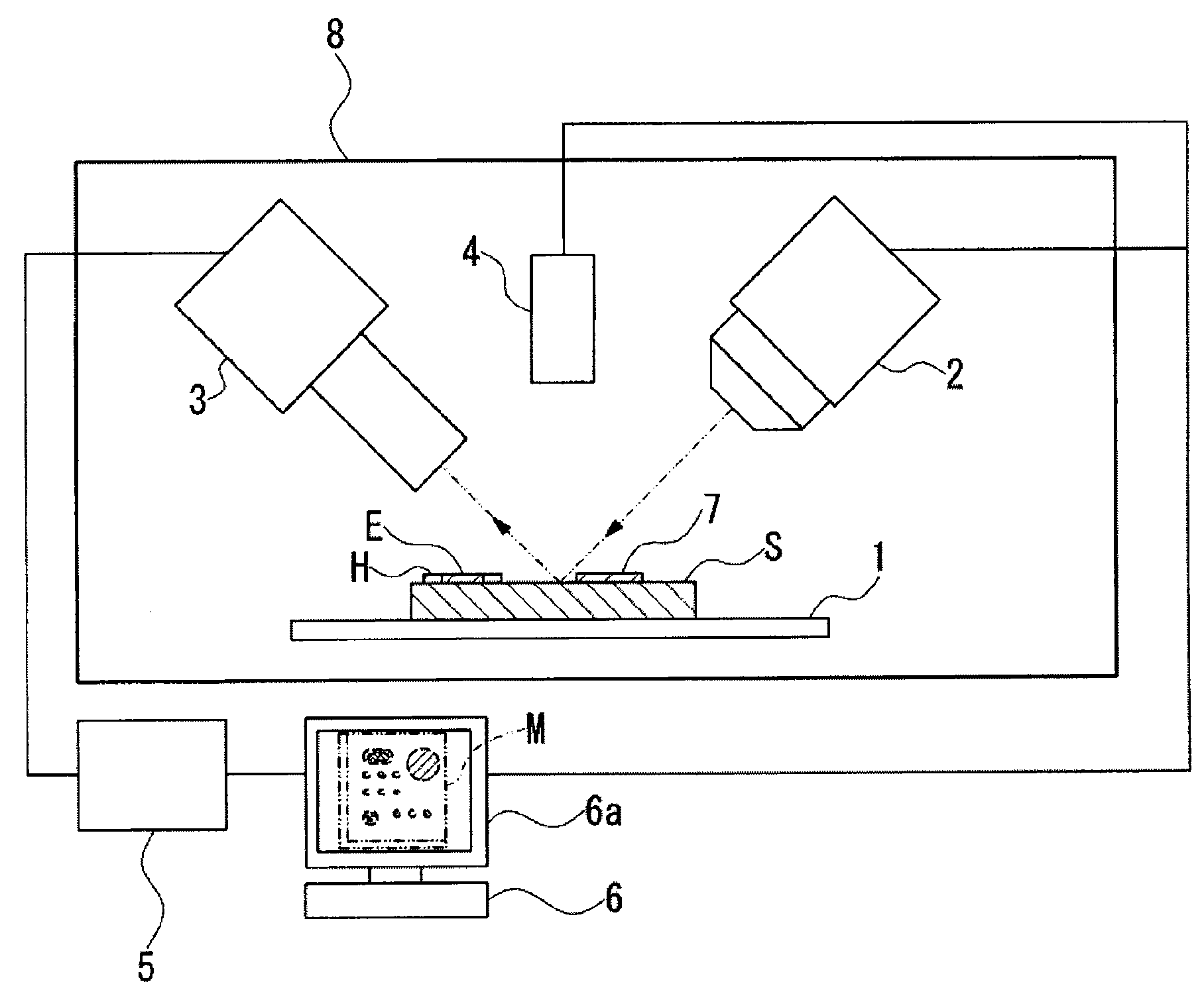
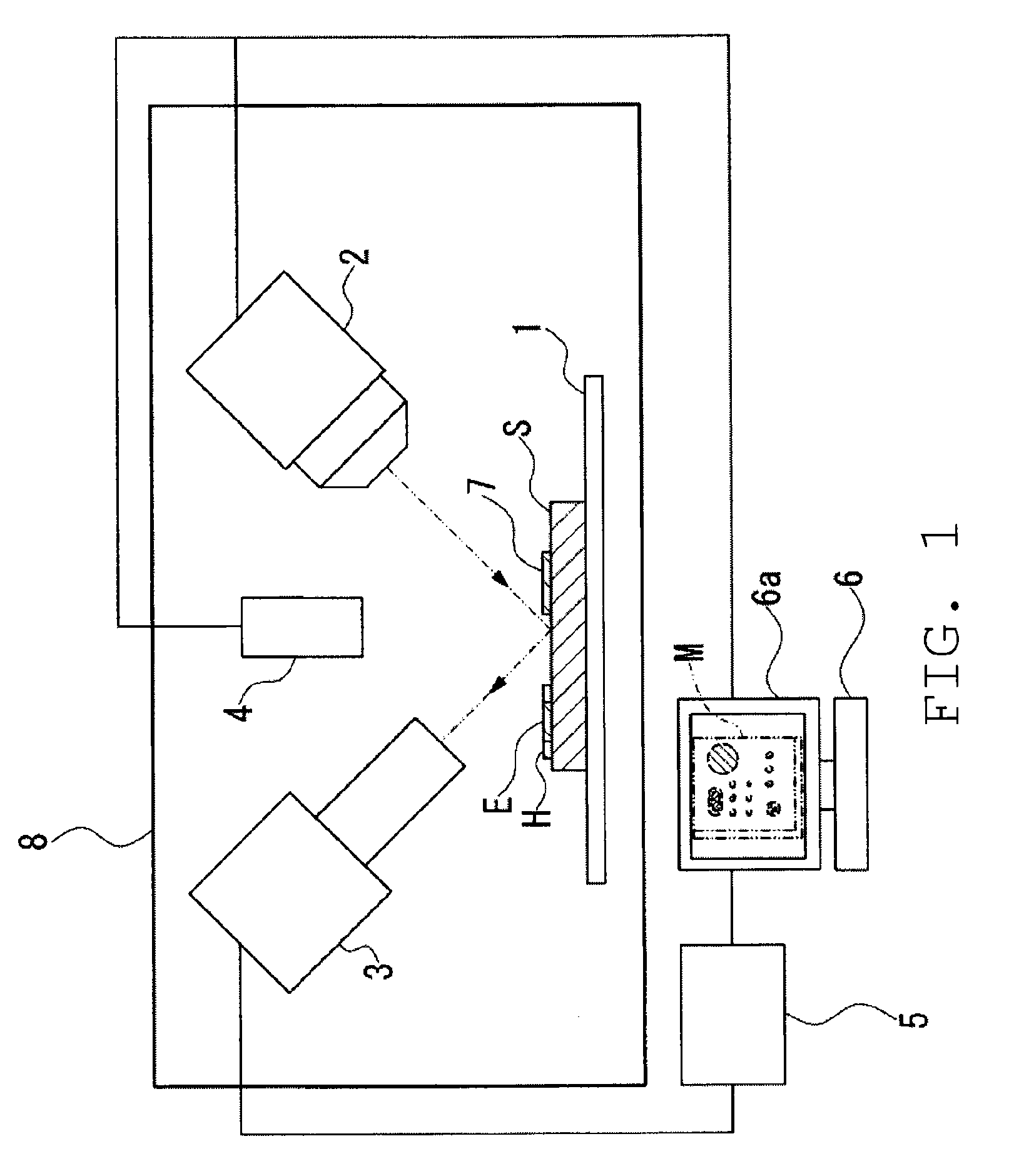
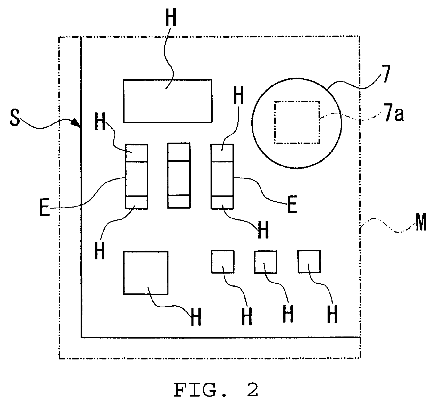
- An X-ray analysis apparatus and method that includes a radiation source, detector, analyzer, and X-ray mapping processing section, which uses a reference material with known component elements and concentrations to determine intensity contrast and display X-ray intensity, allowing for easy visualization of element distribution by comparing with the reference material, and optionally superimposing optical microscope or secondary electron images.

X-ray diffraction and X-ray spectroscopy method and related apparatus
PatentInactiveUS11105756B2
Innovation
- A system utilizing a white X-ray beam and a two-dimensional energy dispersive detector with an array of pixels to simultaneously collect and analyze X-ray diffraction and spectroscopy signals, employing a controller to separate, correct, and sum the signals for enhanced spectra, allowing for rapid determination of material structure and composition without mechanical movement.


Safety Standards for X-ray Equipment Operations
X-ray diffraction equipment used for precise elemental mapping operates under stringent safety frameworks established by multiple international and national regulatory bodies. The International Electrotechnical Commission (IEC) provides foundational standards through IEC 60601-2-28, which specifically addresses radiation safety requirements for X-ray equipment in analytical applications. These standards mandate comprehensive radiation shielding protocols, ensuring that exposure levels remain well below occupational limits of 20 mSv per year for radiation workers and 1 mSv per year for the general public.
Operational safety protocols for XRD elemental mapping systems require multi-layered protection mechanisms. Primary safety features include interlocked sample chambers that automatically shut down X-ray generation when opened, lead-lined enclosures with minimum thickness specifications based on tube voltage and current, and mandatory radiation monitoring systems. Personnel must undergo specialized training covering radiation physics, equipment operation procedures, and emergency response protocols before operating high-resolution mapping systems.
Equipment certification processes involve rigorous testing by authorized bodies such as the Food and Drug Administration (FDA) in the United States and corresponding agencies in other jurisdictions. Manufacturers must demonstrate compliance with leakage radiation limits, typically not exceeding 0.1% of the useful beam intensity at one meter from the electron path. Regular calibration and maintenance schedules are mandated, with quarterly radiation surveys and annual comprehensive safety assessments required for most installations.
Modern XRD systems incorporate advanced safety technologies including real-time radiation monitoring with automatic shutdown capabilities, redundant interlock systems, and sophisticated beam conditioning apparatus. Emergency procedures must be clearly documented and regularly practiced, covering scenarios such as equipment malfunction, radiation exposure incidents, and sample containment breaches. These comprehensive safety frameworks ensure that precise elemental mapping applications can be conducted with minimal risk to operators and surrounding personnel while maintaining analytical accuracy and reliability.
Data Processing Algorithms for XRD Mapping Analysis
Data processing algorithms form the computational backbone of XRD mapping analysis, transforming raw diffraction patterns into meaningful elemental distribution maps. These algorithms must handle massive datasets generated by modern XRD mapping systems, which can produce thousands of diffraction patterns per sample, each containing hundreds to thousands of data points across different diffraction angles.
Peak identification and fitting algorithms represent the first critical processing step. Advanced pattern recognition techniques, including machine learning-based approaches, automatically identify characteristic diffraction peaks within noisy datasets. Sophisticated fitting algorithms, such as pseudo-Voigt functions and asymmetric peak models, accurately determine peak positions, intensities, and widths. These parameters directly correlate to elemental concentrations and crystallographic properties at each mapped position.
Phase identification algorithms utilize comprehensive crystallographic databases to match observed diffraction patterns with known crystal structures. Modern approaches employ probabilistic matching algorithms and artificial intelligence techniques to handle complex multi-phase samples and overlapping peaks. These algorithms must account for preferred orientation effects, strain-induced peak shifts, and instrumental broadening to ensure accurate phase assignments.
Quantitative analysis algorithms convert peak intensities into elemental concentrations using Rietveld refinement methods and reference intensity ratio techniques. These algorithms incorporate correction factors for absorption effects, particle size variations, and texture influences. Advanced implementations utilize iterative refinement procedures to optimize structural parameters and improve quantification accuracy across the entire mapped area.
Spatial correlation algorithms process the positional information to generate high-resolution elemental maps. Interpolation techniques, including kriging and spline-based methods, enhance spatial resolution between measurement points. Noise reduction algorithms, such as principal component analysis and wavelet filtering, improve map quality while preserving essential spatial features and elemental boundaries.
Real-time processing capabilities have become increasingly important for industrial applications. Parallel computing architectures and GPU-accelerated algorithms enable near-instantaneous data processing, allowing for immediate feedback during measurement campaigns. These implementations optimize memory usage and computational efficiency to handle the substantial data throughput requirements of modern XRD mapping systems.
Unlock deeper insights with PatSnap Eureka Quick Research — get a full tech report to explore trends and direct your research. Try now!
Generate Your Research Report Instantly with AI Agent
Supercharge your innovation with PatSnap Eureka AI Agent Platform!