Compact, Low-cost Piezoelectric Sensors for Consumer Markets
JUL 17, 20259 MIN READ
Generate Your Research Report Instantly with AI Agent
Patsnap Eureka helps you evaluate technical feasibility & market potential.
Piezoelectric Sensor Evolution and Objectives
Piezoelectric sensors have undergone significant evolution since their inception in the early 20th century. Initially developed for sonar applications during World War I, these sensors have since found their way into numerous consumer and industrial applications. The technology's journey has been marked by continuous improvements in materials, manufacturing processes, and miniaturization techniques.
In the 1950s and 1960s, the discovery of new piezoelectric materials, such as lead zirconate titanate (PZT), revolutionized the field. These materials offered superior piezoelectric properties, enabling the development of more sensitive and efficient sensors. The subsequent decades saw further advancements in ceramic processing and thin-film deposition techniques, allowing for the production of smaller, more precise sensors.
The 1980s and 1990s witnessed a surge in consumer electronics applications, driving the need for compact and cost-effective piezoelectric sensors. This period saw the integration of these sensors into various devices, from automotive systems to household appliances. The miniaturization trend continued into the 21st century, with the emergence of microelectromechanical systems (MEMS) technology further reducing sensor size and cost.
Today, the focus of piezoelectric sensor development is on creating ultra-compact, low-cost solutions suitable for mass-market consumer applications. The primary objectives of current research include:
1. Size reduction: Developing sensors that can be easily integrated into small consumer devices without compromising performance.
2. Cost optimization: Exploring new materials and manufacturing processes to reduce production costs and make sensors more accessible for widespread consumer use.
3. Energy efficiency: Improving the energy harvesting capabilities of piezoelectric sensors to enable self-powered devices and extend battery life in portable electronics.
4. Sensitivity enhancement: Increasing the sensors' ability to detect minute vibrations or pressure changes, expanding their potential applications in consumer products.
5. Durability and reliability: Enhancing the longevity and stability of sensors to withstand the rigors of everyday consumer use.
6. Multi-functionality: Developing sensors that can serve multiple purposes within a single device, such as combining touch sensing with energy harvesting capabilities.
These objectives align with the growing demand for smart, connected devices in the Internet of Things (IoT) era. As consumer markets continue to evolve, piezoelectric sensors are poised to play a crucial role in enabling new functionalities and improving user experiences across a wide range of products.
Consumer Market Demand Analysis
The consumer market for compact, low-cost piezoelectric sensors is experiencing significant growth, driven by the increasing demand for smart devices and Internet of Things (IoT) applications. These sensors, capable of converting mechanical stress into electrical signals, are finding widespread adoption in various consumer electronics, home automation systems, and wearable devices.
In the smartphone industry, piezoelectric sensors are being integrated into advanced haptic feedback systems, enhancing user experience through more precise and responsive touch sensations. The market for these sensors in smartphones is expected to expand as manufacturers seek to differentiate their products with improved tactile interfaces.
Wearable technology represents another burgeoning sector for piezoelectric sensors. Fitness trackers, smartwatches, and health monitoring devices utilize these sensors to measure physical activities, heart rate, and other biometric data. As consumers become more health-conscious, the demand for accurate and reliable wearable devices is projected to drive the adoption of compact piezoelectric sensors.
In the smart home ecosystem, piezoelectric sensors are finding applications in security systems, energy management, and home automation. These sensors can detect vibrations, movements, and pressure changes, enabling features such as intrusion detection, occupancy sensing, and gesture control interfaces. The growing trend of home automation and the increasing popularity of voice-activated smart home devices are creating new opportunities for piezoelectric sensor integration.
The automotive industry is also contributing to the demand for compact piezoelectric sensors in consumer markets. Advanced driver assistance systems (ADAS) and in-vehicle infotainment systems are incorporating these sensors for various functions, including touchless gesture control and occupant detection. As vehicles become more connected and autonomous, the need for reliable and cost-effective sensing technologies is expected to grow.
Consumer appliances and white goods are another area where piezoelectric sensors are gaining traction. These sensors are being used in washing machines for load balancing, in refrigerators for door open/close detection, and in air conditioners for airflow monitoring. The trend towards smart appliances and energy-efficient products is driving the integration of these sensors to improve functionality and user experience.
The gaming and virtual reality (VR) markets present additional opportunities for compact piezoelectric sensors. These sensors can enhance the immersive experience in VR headsets and gaming controllers by providing more accurate motion tracking and haptic feedback. As the gaming industry continues to evolve, the demand for high-performance, low-latency sensors is expected to increase.
Overall, the consumer market demand for compact, low-cost piezoelectric sensors is multifaceted and growing across various product categories. The key drivers include the need for improved user interfaces, enhanced functionality in smart devices, and the ongoing trend of miniaturization in consumer electronics. As technology advances and manufacturing processes become more efficient, the market is likely to see further expansion, with new applications emerging in response to evolving consumer preferences and technological capabilities.
Current Challenges in Miniaturization
The miniaturization of piezoelectric sensors for consumer markets presents several significant challenges. One of the primary obstacles is maintaining sensor performance while reducing size. As dimensions decrease, the piezoelectric effect becomes less pronounced, potentially compromising sensitivity and signal-to-noise ratio. This necessitates innovative material engineering and design strategies to optimize performance at smaller scales.
Another critical challenge lies in the integration of these compact sensors into consumer devices. Miniaturization often requires redesigning the sensor's form factor and connection interfaces, which can complicate manufacturing processes and increase production costs. Ensuring compatibility with existing electronic components and manufacturing techniques while reducing size is a delicate balancing act.
The quest for cost-effectiveness in miniaturization poses its own set of hurdles. Smaller sensors often require more precise manufacturing techniques and higher-grade materials, which can drive up production expenses. Striking a balance between miniaturization and cost-efficiency is crucial for widespread adoption in consumer markets, where price sensitivity is a key factor.
Thermal management becomes increasingly complex as sensor size decreases. Compact designs leave less room for heat dissipation, potentially affecting sensor accuracy and longevity. Developing effective thermal management solutions without significantly increasing size or cost is a persistent challenge in miniaturization efforts.
Power consumption is another critical consideration. While smaller sensors generally require less power, the reduced surface area can limit energy harvesting capabilities in self-powered designs. Optimizing power efficiency while maintaining functionality in compact form factors is essential for battery-powered consumer devices.
Durability and reliability present additional challenges in miniaturization. Smaller components may be more susceptible to mechanical stress and environmental factors. Ensuring robust performance and longevity in diverse consumer applications requires innovative packaging and protection strategies that do not significantly increase overall size.
Lastly, the challenge of scalability in manufacturing cannot be overlooked. Transitioning from prototype to mass production of miniaturized sensors demands highly precise and consistent manufacturing processes. Developing scalable production methods that maintain quality while keeping costs low is crucial for successful commercialization in consumer markets.
Existing Compact Sensor Solutions
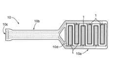
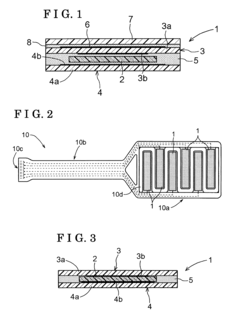
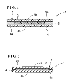
01 Miniaturization of piezoelectric sensors
Advancements in manufacturing techniques have led to the development of smaller piezoelectric sensors. These miniaturized sensors maintain high sensitivity while reducing overall size, making them suitable for various applications where space is limited. The reduced size often correlates with lower material costs, potentially decreasing the overall cost of the sensors.- Miniaturization of piezoelectric sensors: Advancements in manufacturing techniques have led to the development of smaller piezoelectric sensors. These miniaturized sensors maintain high sensitivity while reducing overall size, making them suitable for various applications where space is limited. The reduced size often correlates with lower material costs, potentially decreasing the overall cost of the sensors.
- Cost-effective manufacturing processes: Innovative manufacturing processes have been developed to reduce the production costs of piezoelectric sensors. These methods include improved material deposition techniques, automated assembly processes, and the use of alternative, less expensive piezoelectric materials. These advancements contribute to making piezoelectric sensors more economically viable for widespread use.
- Integration of piezoelectric sensors in MEMS devices: The integration of piezoelectric sensors into Micro-Electro-Mechanical Systems (MEMS) has led to significant reductions in both size and cost. This approach allows for the fabrication of multiple sensors on a single chip, reducing manufacturing costs and enabling the creation of compact, multi-functional sensing devices.
- Use of novel piezoelectric materials: Research into new piezoelectric materials has resulted in the development of sensors with improved performance characteristics and potentially lower costs. These materials may offer better sensitivity, wider operating temperature ranges, or enhanced durability, while also being more cost-effective to produce or process compared to traditional piezoelectric materials.
- Application-specific sensor designs: Tailoring piezoelectric sensor designs for specific applications has led to optimized size and cost profiles. By focusing on the essential requirements of a particular use case, unnecessary features can be eliminated, resulting in more compact and cost-effective sensor solutions. This approach has enabled the development of specialized sensors for various industries and applications.
02 Cost-effective manufacturing processes
Innovative manufacturing processes have been developed to reduce the production costs of piezoelectric sensors. These include improved material deposition techniques, automated assembly methods, and the use of alternative, less expensive piezoelectric materials. Such advancements contribute to making piezoelectric sensors more economically viable for widespread use.Expand Specific Solutions03 Integration of piezoelectric sensors in MEMS devices
Micro-Electro-Mechanical Systems (MEMS) technology has enabled the integration of piezoelectric sensors into compact, multi-functional devices. This integration allows for the creation of smaller, more efficient sensor systems that can be produced at a lower cost due to batch fabrication processes.Expand Specific Solutions04 Use of novel piezoelectric materials
Research into new piezoelectric materials has led to the discovery of compounds with improved properties, such as higher sensitivity and lower power consumption. These novel materials can potentially reduce the size and cost of piezoelectric sensors while enhancing their performance.Expand Specific Solutions05 Application-specific sensor designs
Tailoring piezoelectric sensor designs for specific applications has resulted in optimized size and cost profiles. By focusing on the essential requirements for each application, unnecessary features can be eliminated, leading to more compact and cost-effective sensor solutions.Expand Specific Solutions
Key Players in Sensor Industry
The market for compact, low-cost piezoelectric sensors in consumer markets is in a growth phase, driven by increasing demand for smart devices and IoT applications. The global market size is expanding rapidly, with projections indicating significant growth in the coming years. Technologically, while piezoelectric sensors are well-established, innovations in miniaturization and cost reduction are ongoing. Key players like Murata Manufacturing, Honeywell, and Seiko Epson are leading the field, with companies such as Texas Instruments and Fraunhofer-Gesellschaft contributing to advancements. The competitive landscape is characterized by a mix of established electronics manufacturers and specialized sensor companies, all vying to develop more efficient and affordable solutions for mass-market applications.
Murata Manufacturing Co. Ltd.
Technical Solution: Murata has developed ultra-compact piezoelectric sensors using MEMS technology. Their approach involves creating multilayer ceramic capacitors (MLCCs) with integrated piezoelectric elements, allowing for miniaturization while maintaining high sensitivity. The company has achieved sensors as small as 1.0 x 0.5 x 0.5 mm, suitable for wearable devices and IoT applications[1]. Murata's sensors utilize advanced materials like lead zirconate titanate (PZT) and aluminum nitride (AlN) to optimize performance in small form factors. They have also implemented innovative packaging techniques, such as wafer-level packaging, to further reduce costs and size[2].
Strengths: Industry-leading miniaturization, high-volume production capabilities, and extensive experience in ceramic components. Weaknesses: Reliance on some rare earth materials may impact long-term cost-effectiveness.
Texas Instruments Incorporated
Technical Solution: Texas Instruments has focused on developing integrated solutions for piezoelectric sensor interfaces. Their approach combines low-power analog front-end (AFE) circuits with high-resolution analog-to-digital converters (ADCs) optimized for piezoelectric sensor signals. TI's PGA460 ultrasonic sensor-signal conditioner is an example of this integration, featuring a programmable gain amplifier and 12-bit ADC in a single chip[3]. They have also developed energy harvesting circuits that can power sensors from piezoelectric vibrations, potentially eliminating the need for batteries in some applications[4]. TI's emphasis on power efficiency and integration helps reduce overall system cost and size for consumer applications.
Strengths: Strong expertise in mixed-signal integration and low-power design. Comprehensive ecosystem of supporting components. Weaknesses: Less focus on the sensor element itself, relying more on third-party sensors.
Core Innovations in Materials
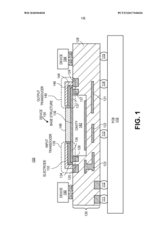
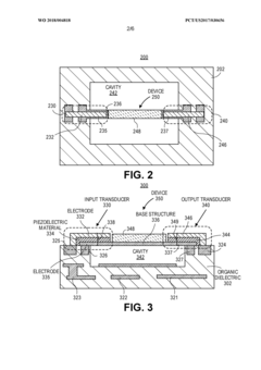
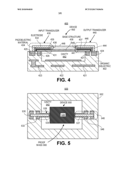
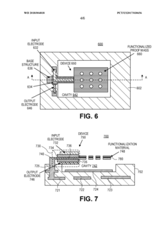
Piezoelectric package-integrated chemical species-sensitive resonant devices
PatentWO2018004818A1
Innovation
- The development of package-integrated piezoelectric chemical species-sensitive resonant devices, which are fabricated as part of the organic package substrate, utilizing suspended structures mechanically coupled to piezoelectric materials, allowing for direct integration and lower-cost high-volume manufacturing, with enhanced sensitivity and selectivity through the deposition and crystallization of high-quality piezoelectric thin films without degrading the substrate.
Piezoelectric sensor and method for manufacturing the same
PatentInactiveUS20090289529A1
Innovation
- The piezoelectric sensor design features a polymeric piezoelectric body supported between insulating layers with overlapping signal and ground electrodes, reducing piezoelectric body consumption and noise, and using insulating films to support electrodes, which allows for efficient production and improved sensitivity by fixing the electrodes directly to the piezoelectric body via a fixative.
Cost Reduction Techniques
Cost reduction techniques for piezoelectric sensors in consumer markets focus on optimizing materials, manufacturing processes, and design strategies. One key approach is the use of alternative piezoelectric materials. While traditional lead zirconate titanate (PZT) remains widely used, research into lead-free alternatives like barium titanate (BaTiO3) and potassium sodium niobate (KNN) shows promise for reducing material costs while maintaining performance.
Miniaturization plays a crucial role in cost reduction. By shrinking sensor dimensions, manufacturers can reduce material usage and increase the number of sensors produced per wafer. Advanced microfabrication techniques, such as thin-film deposition and etching processes, enable the creation of compact sensors with reduced material consumption.
Integration of multiple functions into a single sensor package can significantly lower overall costs. For instance, combining sensing elements with signal conditioning circuitry in a single chip reduces assembly complexity and component count. This approach, known as system-on-chip (SoC) or system-in-package (SiP), minimizes packaging costs and improves reliability.
Automation and streamlined manufacturing processes contribute substantially to cost reduction. Implementation of high-volume production techniques, such as roll-to-roll processing for flexible sensors, can dramatically decrease per-unit costs. Additionally, adopting standardized designs and modular components across product lines enables economies of scale in production.
Novel fabrication methods, like 3D printing of piezoelectric materials, offer potential for reducing manufacturing costs. These additive manufacturing techniques allow for rapid prototyping and customization of sensor designs, potentially lowering development costs and time-to-market for new products.
Optimizing sensor packaging is another avenue for cost reduction. Utilizing low-cost, durable materials for encapsulation and exploring novel packaging techniques can significantly decrease overall sensor costs. For example, implementing wafer-level packaging reduces individual handling steps and associated labor costs.
Lastly, improving yield rates through enhanced quality control measures and process optimization can indirectly contribute to cost reduction. By minimizing defects and waste during production, manufacturers can lower the effective cost per functional sensor unit, making them more accessible for consumer applications.
Environmental Impact Assessment
The environmental impact of compact, low-cost piezoelectric sensors for consumer markets is an important consideration in their development and widespread adoption. These sensors, while offering significant benefits in terms of size and affordability, also present potential environmental challenges throughout their lifecycle.
During the manufacturing process, the production of piezoelectric materials often involves the use of lead-based compounds, which can pose environmental risks if not properly managed. However, recent advancements in lead-free piezoelectric materials are helping to mitigate these concerns. The miniaturization of these sensors also contributes to reduced material consumption and energy usage during production, potentially lowering their overall environmental footprint.
In the usage phase, the compact nature of these sensors contributes to energy efficiency in consumer devices. Their low power requirements can lead to extended battery life in portable electronics, reducing the frequency of battery replacements and associated waste. Additionally, the integration of these sensors into smart home devices and wearable technology can promote energy-saving behaviors and more efficient resource management in households.
However, the increased proliferation of these sensors in consumer products raises concerns about electronic waste (e-waste) at the end of their lifecycle. The small size of these components can make them challenging to recover and recycle, potentially leading to improper disposal. This issue is compounded by the rapid turnover of consumer electronics, which may result in a growing volume of discarded sensors.
To address these environmental challenges, manufacturers are exploring eco-friendly design approaches. This includes the development of biodegradable or easily recyclable sensor components, as well as the implementation of take-back programs to ensure proper disposal and recycling of devices containing these sensors. Furthermore, efforts are being made to improve the durability and lifespan of these sensors, reducing the frequency of replacement and associated waste generation.
The environmental impact of these sensors also extends to their potential applications in environmental monitoring and conservation efforts. Their low cost and compact size make them suitable for widespread deployment in air and water quality monitoring systems, wildlife tracking, and precision agriculture. These applications can contribute to more effective environmental management and resource conservation strategies.
In conclusion, while compact, low-cost piezoelectric sensors offer significant environmental benefits through energy efficiency and potential applications in environmental monitoring, careful consideration must be given to their entire lifecycle impact. Continued research and development in eco-friendly materials, manufacturing processes, and end-of-life management are crucial to maximizing the positive environmental contributions of these sensors while minimizing their negative impacts.
Unlock deeper insights with Patsnap Eureka Quick Research — get a full tech report to explore trends and direct your research. Try now!
Generate Your Research Report Instantly with AI Agent
Supercharge your innovation with Patsnap Eureka AI Agent Platform!