Cutting-edge Surface Engineering for Piezoelectric Sensors
JUL 17, 20259 MIN READ
Generate Your Research Report Instantly with AI Agent
Patsnap Eureka helps you evaluate technical feasibility & market potential.
Piezoelectric Sensor Surface Engineering Overview
Piezoelectric sensors have revolutionized various industries with their ability to convert mechanical stress into electrical signals. The surface engineering of these sensors plays a crucial role in enhancing their performance, reliability, and longevity. This overview explores the cutting-edge developments in surface engineering techniques for piezoelectric sensors.
Surface engineering for piezoelectric sensors encompasses a wide range of processes and technologies aimed at modifying the sensor's surface properties. These modifications can significantly impact the sensor's sensitivity, response time, and overall functionality. Advanced coating techniques, such as physical vapor deposition (PVD) and chemical vapor deposition (CVD), have emerged as powerful tools for creating ultra-thin, uniform layers on sensor surfaces.
Nanostructured coatings have gained considerable attention in recent years. These coatings, often composed of materials like titanium dioxide or zinc oxide, can dramatically increase the surface area of the sensor, leading to enhanced sensitivity and faster response times. Additionally, the use of nanoparticles in surface treatments has shown promise in improving the sensor's resistance to environmental factors such as humidity and temperature fluctuations.
Another area of focus in piezoelectric sensor surface engineering is the development of self-cleaning and anti-fouling coatings. These innovative surfaces can maintain the sensor's performance over extended periods by preventing the accumulation of contaminants. Hydrophobic and oleophobic coatings, inspired by natural surfaces like lotus leaves, are being explored to create sensors that remain clean and functional in challenging environments.
The integration of smart materials in surface engineering is opening new possibilities for piezoelectric sensors. Shape memory alloys and phase-change materials are being investigated for their potential to create adaptive sensor surfaces that can respond to environmental changes. This adaptability could lead to sensors with broader operating ranges and improved accuracy across various conditions.
Biomimetic approaches to surface engineering are also gaining traction. Researchers are drawing inspiration from natural structures, such as the intricate patterns on butterfly wings or the adhesive properties of gecko feet, to create sensor surfaces with enhanced properties. These bio-inspired designs could lead to sensors with improved sensitivity, durability, and even self-healing capabilities.
As the field of piezoelectric sensor surface engineering continues to evolve, interdisciplinary collaboration between materials scientists, engineers, and biologists is driving innovation. The convergence of nanotechnology, smart materials, and biomimetics is paving the way for next-generation sensors with unprecedented performance characteristics. These advancements are expected to expand the application of piezoelectric sensors in fields ranging from healthcare and environmental monitoring to aerospace and industrial automation.
Market Demand Analysis
The market demand for advanced surface engineering in piezoelectric sensors has been experiencing significant growth, driven by the increasing adoption of these sensors across various industries. Piezoelectric sensors, known for their ability to convert mechanical stress into electrical signals, are finding widespread applications in automotive, healthcare, industrial, and consumer electronics sectors.
In the automotive industry, there is a growing demand for piezoelectric sensors with enhanced surface properties to improve fuel efficiency, emissions control, and overall vehicle performance. These sensors are crucial in engine management systems, tire pressure monitoring, and advanced driver assistance systems (ADAS). The automotive sector's shift towards electric and autonomous vehicles is further fueling the need for high-performance piezoelectric sensors with superior surface characteristics.
The healthcare sector presents another substantial market for cutting-edge surface-engineered piezoelectric sensors. These sensors are increasingly used in medical imaging equipment, such as ultrasound machines, where improved surface properties can lead to enhanced image quality and diagnostic accuracy. Additionally, there is a rising demand for miniaturized sensors in wearable health monitoring devices, requiring advanced surface engineering techniques to maintain sensor performance while reducing size.
In the industrial sector, piezoelectric sensors with enhanced surface properties are gaining traction in structural health monitoring, vibration analysis, and process control applications. The need for sensors that can withstand harsh environments and provide accurate measurements in challenging conditions is driving the demand for innovative surface engineering solutions.
The consumer electronics market is another key driver for advanced surface engineering in piezoelectric sensors. With the proliferation of smartphones, tablets, and other portable devices, there is a growing need for sensors with improved durability, sensitivity, and energy efficiency. Surface engineering techniques that can enhance these properties while maintaining cost-effectiveness are highly sought after in this competitive market.
The global market for piezoelectric sensors is projected to grow steadily in the coming years, with surface engineering playing a crucial role in this expansion. As industries continue to demand sensors with higher performance, reliability, and longevity, the focus on cutting-edge surface engineering techniques is expected to intensify. This trend is likely to create opportunities for companies specializing in advanced materials and surface modification technologies, as well as for sensor manufacturers looking to differentiate their products in an increasingly competitive market.
Current Challenges in Surface Engineering
Surface engineering for piezoelectric sensors faces several significant challenges that hinder the advancement and widespread application of these devices. One of the primary obstacles is achieving consistent and uniform surface properties across large areas. The performance of piezoelectric sensors heavily relies on the quality and characteristics of their surface, making it crucial to develop techniques that can produce homogeneous surface properties at scale.
Another major challenge lies in enhancing the durability and longevity of piezoelectric sensor surfaces. These sensors are often exposed to harsh environments, including extreme temperatures, corrosive substances, and mechanical stress. Developing surface engineering techniques that can withstand these conditions while maintaining optimal sensor performance remains a significant hurdle for researchers and engineers in the field.
The integration of multifunctionality into piezoelectric sensor surfaces presents yet another challenge. As the demand for more sophisticated and versatile sensors grows, there is a need to engineer surfaces that can simultaneously exhibit piezoelectric properties, biocompatibility, and other desired characteristics such as self-cleaning or anti-fouling properties. Achieving this level of multifunctionality without compromising the core piezoelectric performance is a complex task that requires innovative approaches and materials.
Nano-scale surface engineering poses its own set of challenges. While nanotechnology offers immense potential for enhancing sensor sensitivity and performance, controlling and manipulating surface structures at the nanometer scale with precision and reproducibility remains difficult. This challenge is further compounded by the need to develop scalable manufacturing processes that can consistently produce these nano-engineered surfaces.
The environmental impact of surface engineering processes is an increasingly important consideration. Many traditional surface treatment methods involve the use of hazardous chemicals or energy-intensive processes. Developing eco-friendly and sustainable surface engineering techniques that maintain or improve upon the performance of piezoelectric sensors is a critical challenge that aligns with global sustainability goals.
Lastly, the characterization and quality control of engineered surfaces present ongoing challenges. As surface engineering techniques become more sophisticated, there is a growing need for advanced analytical tools and methodologies to accurately assess surface properties and ensure consistency in production. This includes developing non-destructive testing methods that can be integrated into manufacturing processes for real-time quality control.
Existing Surface Treatment Solutions
01 Surface acoustic wave (SAW) sensors
Piezoelectric sensors utilizing surface acoustic waves for various sensing applications. These sensors exploit the propagation of acoustic waves along the surface of a piezoelectric material to detect changes in physical properties or the presence of specific substances.- Surface acoustic wave (SAW) sensors: Surface acoustic wave sensors utilize piezoelectric materials to generate and detect acoustic waves on the surface of a substrate. These sensors are highly sensitive to changes in mass, temperature, and other physical properties, making them suitable for various sensing applications.
- Piezoelectric thin film deposition: The deposition of piezoelectric thin films on various substrates is crucial for creating high-performance sensors. Techniques such as sputtering, sol-gel, and chemical vapor deposition are used to create uniform and well-oriented piezoelectric layers for optimal sensor performance.
- Surface modification for enhanced sensitivity: Modifying the surface of piezoelectric sensors can significantly improve their sensitivity and selectivity. This includes creating nanostructures, applying functional coatings, or introducing specific binding sites on the sensor surface to enhance interaction with target analytes.
- Integration of piezoelectric sensors in MEMS devices: Piezoelectric sensors are increasingly integrated into microelectromechanical systems (MEMS) for various applications. This integration allows for miniaturization, improved performance, and the development of multi-functional sensing platforms.
- Novel piezoelectric materials for sensor applications: Research into new piezoelectric materials aims to improve sensor performance, stability, and compatibility with different environments. This includes the development of lead-free piezoelectrics, composite materials, and nanostructured piezoelectric elements.
02 Thin-film piezoelectric sensors
Development of thin-film piezoelectric sensors for enhanced sensitivity and miniaturization. These sensors use thin layers of piezoelectric materials deposited on various substrates, allowing for integration into compact devices and improved performance in detecting minute forces or vibrations.Expand Specific Solutions03 Surface modification of piezoelectric sensors
Techniques for modifying the surface of piezoelectric sensors to enhance their performance or add functionality. This includes surface treatments, coatings, or patterning to improve sensitivity, selectivity, or durability of the sensor surface.Expand Specific Solutions04 Piezoelectric sensor arrays
Design and fabrication of piezoelectric sensor arrays for multi-point sensing or imaging applications. These arrays consist of multiple piezoelectric elements arranged on a surface to provide spatial resolution in detecting forces, pressures, or vibrations.Expand Specific Solutions05 Integration of piezoelectric sensors with MEMS
Incorporation of piezoelectric sensors into microelectromechanical systems (MEMS) for advanced sensing capabilities. This integration allows for the development of compact, highly sensitive devices that combine the benefits of piezoelectric materials with microfabrication technologies.Expand Specific Solutions
Key Industry Players
The research on cutting-edge surface engineering for piezoelectric sensors is in a growth phase, with increasing market size and technological advancements. The global piezoelectric sensors market is expanding rapidly, driven by applications in automotive, healthcare, and industrial sectors. While the technology is maturing, there's still room for innovation in surface engineering techniques. Key players like Murata Manufacturing, Kyocera, and Robert Bosch are leading the field, with significant contributions from research institutions such as Vanderbilt University and the Luxembourg Institute of Science & Technology. These organizations are focusing on improving sensor performance, durability, and miniaturization through advanced surface engineering methods, indicating a competitive and dynamic landscape in this technological domain.
Murata Manufacturing Co. Ltd.
Technical Solution: Murata has developed advanced surface engineering techniques for piezoelectric sensors, focusing on enhancing sensitivity and durability. They employ thin-film deposition methods, such as sputtering and chemical vapor deposition, to create precise piezoelectric layers on various substrates. Their approach includes the use of novel materials like aluminum nitride (AlN) and scandium-doped aluminum nitride (ScAlN) for improved piezoelectric properties[1]. Murata has also implemented nanostructuring techniques to increase the active surface area of sensors, resulting in enhanced sensitivity and response times. Their research extends to the development of flexible piezoelectric sensors using polymer-based materials and incorporating graphene for improved conductivity and mechanical strength[2].
Strengths: High precision in thin-film deposition, expertise in novel piezoelectric materials, and advanced nanostructuring techniques. Weaknesses: Potential high production costs and complexity in scaling up nanostructured surfaces for mass production.
Kyocera Corp.
Technical Solution: Kyocera has made significant strides in surface engineering for piezoelectric sensors, particularly in the field of high-temperature applications. Their research focuses on developing robust piezoelectric materials and protective coatings that can withstand extreme conditions. Kyocera has pioneered the use of langasite (La3Ga5SiO14) crystals for high-temperature sensing applications, capable of operating at temperatures up to 1000°C[3]. They have also developed specialized surface treatments and electrode designs to enhance the stability and longevity of piezoelectric sensors in harsh environments. Kyocera's approach includes the integration of advanced ceramics and composite materials to create sensors with improved thermal and mechanical properties[4].
Strengths: Expertise in high-temperature piezoelectric materials and protective coatings, robust sensor designs for harsh environments. Weaknesses: Potentially limited applicability in low-cost consumer electronics due to focus on specialized, high-performance applications.
Innovative Surface Engineering Techniques
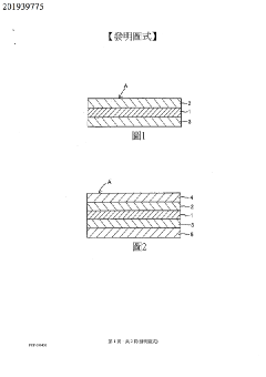
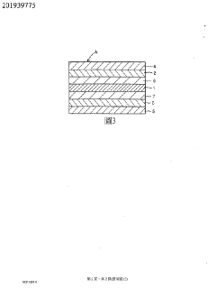
Piezoelectric sensor and method for manufacturing same
PatentActiveEP3726595A1
Innovation
- A flexible piezoelectric sensor design featuring an elongated-sheet shape with a piezoelectric layer and electrode layers containing elastomers and flaky conductive materials, allowing for high conductivity and flexibility, with electrical resistance maintained below 3,000 Ω over a 500 mm pressure sensing region, ensuring accurate detection of weak vibrations and heartbeats without user discomfort.
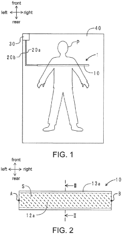
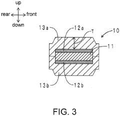


Piezoelectric sensor capable of smoothly following extension of measured body and precisely measuring movement of measured body
PatentActiveTW201939775A
Innovation
- Flexible piezoelectric sensor design using a porous synthetic resin sheet as the piezoelectric element, allowing smooth following of the measured body's extension.
- Incorporation of flexible adhesive resin with conductive particles in both signal and grounding electrode layers, enhancing overall sensor flexibility.
- Layered structure design with piezoelectric sheet sandwiched between signal and grounding electrode layers, enabling precise movement detection on the surface direction.
Environmental Impact Assessment
The environmental impact of cutting-edge surface engineering for piezoelectric sensors is a critical consideration in the development and implementation of these advanced technologies. Surface engineering techniques, such as thin film deposition, plasma treatment, and nanostructuring, can significantly enhance the performance and durability of piezoelectric sensors. However, these processes may also have potential environmental implications that need to be carefully assessed.
One of the primary environmental concerns associated with surface engineering for piezoelectric sensors is the use of hazardous materials and chemicals. Many advanced coating processes involve the application of potentially toxic substances, including heavy metals and volatile organic compounds (VOCs). These materials can pose risks to both human health and the environment if not properly managed throughout the manufacturing, use, and disposal stages of the sensor lifecycle.
Energy consumption is another important factor to consider in the environmental impact assessment of surface engineering processes. High-tech deposition techniques, such as physical vapor deposition (PVD) and chemical vapor deposition (CVD), often require significant energy inputs. This increased energy demand can contribute to greenhouse gas emissions and overall carbon footprint if not sourced from renewable energy sources.
Water usage and potential contamination are also key environmental concerns in surface engineering processes. Some techniques may require substantial amounts of water for cooling or cleaning purposes, potentially straining local water resources. Additionally, wastewater from these processes may contain pollutants that require specialized treatment before release into the environment.
The production of waste materials, including spent chemicals, used filters, and discarded substrates, is an inevitable byproduct of surface engineering processes. Proper disposal and recycling of these materials are essential to minimize environmental impact and comply with regulatory requirements. Implementing circular economy principles in the manufacturing process can help reduce waste generation and improve resource efficiency.
On the positive side, advanced surface engineering techniques can potentially lead to more efficient and longer-lasting piezoelectric sensors. This increased durability and performance can result in reduced material consumption and waste generation over the long term, as fewer sensors need to be produced and replaced. Furthermore, improved sensor efficiency may lead to energy savings in the applications where these sensors are deployed, potentially offsetting some of the environmental impacts associated with their production.
As the field of surface engineering for piezoelectric sensors continues to evolve, there is a growing emphasis on developing more environmentally friendly processes and materials. This includes research into bio-based coatings, low-temperature deposition techniques, and the use of non-toxic alternatives to traditional materials. These advancements aim to mitigate the environmental impact of surface engineering while maintaining or enhancing sensor performance.
Standardization and Quality Control
Standardization and quality control are crucial aspects in the development and production of cutting-edge piezoelectric sensors with advanced surface engineering. The implementation of rigorous standards and quality control measures ensures consistent performance, reliability, and reproducibility of these sensors across various applications.
To establish effective standardization, industry-wide guidelines must be developed for surface engineering techniques specific to piezoelectric sensors. These standards should encompass material selection, surface preparation methods, coating processes, and post-treatment procedures. Collaboration between research institutions, manufacturers, and regulatory bodies is essential to create comprehensive and universally accepted standards.
Quality control in surface engineering for piezoelectric sensors involves multiple stages of inspection and testing. Initial material characterization is critical to ensure the purity and composition of piezoelectric materials and surface coatings. Non-destructive testing methods, such as X-ray diffraction and atomic force microscopy, can be employed to assess surface morphology and crystalline structure.
Process control during surface engineering is vital to maintain consistency. This includes monitoring and controlling parameters such as temperature, pressure, and deposition rates in coating processes. In-situ monitoring techniques, like ellipsometry or quartz crystal microbalance, can provide real-time feedback on coating thickness and uniformity.
Post-processing quality control involves rigorous testing of the engineered surfaces. This includes adhesion tests, wear resistance evaluations, and environmental stability assessments. Electrical characterization of the sensors, including measurements of piezoelectric coefficients and frequency response, is essential to verify the impact of surface engineering on sensor performance.
Statistical process control (SPC) techniques should be implemented to track and analyze key quality indicators over time. This allows for early detection of process drift and enables continuous improvement of surface engineering techniques. Advanced data analytics and machine learning algorithms can be employed to identify correlations between process parameters and final sensor performance, facilitating predictive quality control.
Traceability is another critical aspect of quality control in surface-engineered piezoelectric sensors. Detailed documentation of materials, processes, and test results for each sensor batch ensures accountability and aids in troubleshooting and product improvement. Implementation of digital tracking systems and unique identifiers for each sensor can enhance traceability throughout the production and deployment lifecycle.
Unlock deeper insights with Patsnap Eureka Quick Research — get a full tech report to explore trends and direct your research. Try now!
Generate Your Research Report Instantly with AI Agent
Supercharge your innovation with Patsnap Eureka AI Agent Platform!