Integrated Electronics using Borosilicate Glass Substrates
JUL 3, 20259 MIN READ
Generate Your Research Report Instantly with AI Agent
PatSnap Eureka helps you evaluate technical feasibility & market potential.
Borosilicate Glass in Electronics: Background and Objectives
Borosilicate glass has emerged as a promising material in the field of integrated electronics, offering unique properties that address several challenges in modern electronic device fabrication. This research focuses on exploring the potential of borosilicate glass substrates for integrated electronics, aiming to leverage its advantageous characteristics to enhance device performance and reliability.
The evolution of electronic devices has been marked by a continuous drive towards miniaturization, increased functionality, and improved performance. Traditional substrate materials, such as silicon and various polymers, have limitations in terms of thermal stability, electrical insulation, and compatibility with certain fabrication processes. Borosilicate glass, known for its excellent thermal and chemical resistance, as well as its superior electrical insulating properties, presents an opportunity to overcome these limitations.
Historically, borosilicate glass has been widely used in laboratory glassware and household items due to its low thermal expansion coefficient and high resistance to thermal shock. Its application in electronics has been limited, primarily confined to specialized applications such as microfluidic devices and MEMS (Micro-Electro-Mechanical Systems). However, recent advancements in glass processing technologies have opened up new possibilities for its use in integrated electronics.
The primary objective of this research is to investigate the feasibility and potential benefits of using borosilicate glass as a substrate material for integrated electronic devices. This includes exploring its compatibility with various fabrication processes, such as thin-film deposition, etching, and bonding techniques commonly used in semiconductor manufacturing. Additionally, the research aims to evaluate the performance characteristics of electronic components fabricated on borosilicate glass substrates, focusing on aspects such as thermal management, signal integrity, and long-term reliability.
Another key goal is to identify and develop novel applications that can uniquely benefit from the properties of borosilicate glass. This may include high-frequency electronic devices, where the low dielectric loss of glass can be advantageous, or in harsh environment applications where the chemical and thermal stability of borosilicate glass can enhance device longevity.
Furthermore, this research seeks to address the challenges associated with integrating borosilicate glass into existing electronic manufacturing processes. This involves developing new or modified fabrication techniques that are compatible with glass substrates, as well as exploring methods to enhance the adhesion of various materials to the glass surface.
By comprehensively examining the potential of borosilicate glass in integrated electronics, this research aims to contribute to the advancement of electronic device technology, potentially opening new avenues for innovation in areas such as flexible electronics, high-performance computing, and robust sensing devices for extreme environments.
Market Analysis for Glass-based Integrated Electronics
The market for glass-based integrated electronics is experiencing significant growth, driven by the increasing demand for advanced electronic devices across various industries. Borosilicate glass substrates offer unique properties that make them particularly suitable for integrated electronics applications, including high thermal stability, excellent electrical insulation, and superior optical transparency.
The global market for glass-based integrated electronics is projected to expand rapidly in the coming years, with a compound annual growth rate (CAGR) expected to exceed that of traditional silicon-based electronics. This growth is primarily fueled by the rising adoption of glass substrates in emerging technologies such as flexible displays, wearable devices, and Internet of Things (IoT) sensors.
One of the key drivers of market demand is the consumer electronics sector, where glass-based integrated electronics are being increasingly utilized in smartphones, tablets, and smartwatches. The automotive industry is another significant market, with glass substrates finding applications in advanced driver assistance systems (ADAS) and in-vehicle infotainment systems.
The healthcare sector is also showing growing interest in glass-based integrated electronics, particularly for medical imaging devices and biosensors. The ability of borosilicate glass to withstand sterilization processes and its biocompatibility make it an attractive option for medical applications.
In terms of regional market distribution, Asia-Pacific is expected to dominate the glass-based integrated electronics market, with countries like China, Japan, and South Korea leading in both production and consumption. North America and Europe are also significant markets, driven by their strong presence in the semiconductor and electronics industries.
The market is characterized by intense competition among key players, including major glass manufacturers and electronics companies. These companies are investing heavily in research and development to improve the performance and cost-effectiveness of glass-based integrated electronics.
Despite the positive outlook, the market faces challenges such as high initial production costs and the need for specialized manufacturing processes. However, ongoing technological advancements and economies of scale are expected to gradually address these issues, further driving market growth.
As the technology matures and becomes more cost-effective, new applications are likely to emerge, potentially expanding the market into areas such as energy harvesting devices, advanced optoelectronics, and next-generation computing systems. This diversification of applications is expected to contribute significantly to the long-term growth and sustainability of the glass-based integrated electronics market.
Current Challenges in Borosilicate Glass Substrate Integration
The integration of borosilicate glass substrates in electronics faces several significant challenges that hinder widespread adoption and optimal performance. One of the primary obstacles is the difficulty in achieving reliable and robust bonding between the glass substrate and other materials, such as metals or semiconductors. The difference in thermal expansion coefficients between borosilicate glass and these materials can lead to stress and potential delamination during thermal cycling, compromising the integrity of the integrated system.
Another critical challenge lies in the precise patterning and etching of borosilicate glass substrates. While traditional photolithography techniques work well for silicon-based substrates, they often require modifications when applied to glass. The transparency and non-conductive nature of borosilicate glass can affect the accuracy of pattern transfer and the uniformity of etching processes, leading to potential issues in device fabrication and performance.
The integration of active components, such as transistors or sensors, directly onto borosilicate glass substrates presents additional complexities. The relatively high processing temperatures required for many semiconductor fabrication steps can cause warping or deformation of the glass substrate, necessitating the development of low-temperature processes or alternative integration methods.
Furthermore, the electrical properties of borosilicate glass pose challenges for certain electronic applications. While its low dielectric constant can be advantageous for high-frequency applications, the insulating nature of glass can complicate the creation of conductive pathways and interconnects. This necessitates the development of specialized techniques for metallization and the formation of through-glass vias (TGVs) to enable vertical integration and 3D packaging solutions.
The mechanical fragility of thin borosilicate glass substrates also presents challenges in handling and processing. As the demand for thinner and more flexible electronic devices grows, the risk of breakage during manufacturing and assembly increases, requiring the development of specialized handling equipment and processes to ensure yield and reliability.
Lastly, the cost-effectiveness of borosilicate glass substrate integration remains a significant hurdle. While glass offers several advantages over traditional substrate materials, the specialized processing requirements and potential yield issues can increase manufacturing costs. Balancing the performance benefits with economic viability is crucial for the widespread adoption of this technology in commercial applications.
Existing Integration Methods for Borosilicate Glass Substrates
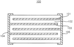
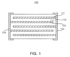
01 Borosilicate glass as a substrate for integrated electronics
Borosilicate glass is used as a substrate material for integrated electronics due to its excellent thermal and chemical stability, low coefficient of thermal expansion, and high transparency. These properties make it suitable for various electronic applications, including display panels, sensors, and microfluidic devices.- Borosilicate glass as a substrate for integrated electronics: Borosilicate glass is used as a substrate material for integrated electronics due to its excellent thermal and chemical stability, low coefficient of thermal expansion, and high transparency. These properties make it suitable for various electronic applications, including display technologies and semiconductor devices.
- Fabrication techniques for borosilicate glass-based electronics: Various fabrication techniques are employed to create integrated electronics on borosilicate glass substrates. These may include thin-film deposition, photolithography, etching processes, and bonding methods. The techniques are optimized to ensure compatibility with the glass substrate and to achieve desired electronic properties.
- Applications of borosilicate glass in electronic devices: Borosilicate glass substrates are used in a wide range of electronic devices, including flat panel displays, touch screens, solar cells, and microfluidic devices. The glass's properties allow for the integration of various electronic components and circuits on a single substrate, enabling the development of compact and efficient devices.
- Surface modification of borosilicate glass for enhanced performance: Surface modification techniques are applied to borosilicate glass substrates to improve their performance in electronic applications. These modifications may include surface activation, coating with functional layers, or creating nanostructures to enhance adhesion, conductivity, or other desired properties.
- Integration of borosilicate glass with other materials: Borosilicate glass is often integrated with other materials to create hybrid electronic structures. This may involve bonding with semiconductors, metals, or polymers to combine the advantages of different materials and achieve specific functionalities in integrated electronic devices.
02 Fabrication techniques for electronics on borosilicate glass
Various fabrication techniques are employed to create integrated electronics on borosilicate glass substrates. These may include photolithography, etching, thin-film deposition, and laser processing. The choice of technique depends on the specific electronic components and the desired functionality of the final device.Expand Specific Solutions03 Surface modification of borosilicate glass for improved adhesion
To enhance the adhesion of electronic components to borosilicate glass substrates, surface modification techniques are employed. These may include plasma treatment, chemical functionalization, or the application of adhesion promoters. Improved adhesion ensures better durability and reliability of the integrated electronic devices.Expand Specific Solutions04 Integration of sensors and actuators on borosilicate glass
Borosilicate glass substrates are used for integrating various sensors and actuators in electronic devices. This includes the fabrication of pressure sensors, temperature sensors, and microelectromechanical systems (MEMS) on the glass surface. The transparency and stability of borosilicate glass make it ideal for these applications.Expand Specific Solutions05 Packaging and encapsulation of electronics on borosilicate glass
Specialized packaging and encapsulation techniques are developed for protecting integrated electronics on borosilicate glass substrates. These methods ensure the longevity and reliability of the electronic components while maintaining the advantages of using glass as a substrate material. Hermetic sealing and advanced bonding techniques are often employed in this process.Expand Specific Solutions
Key Players in Borosilicate Glass and Integrated Electronics
The research on integrated electronics using borosilicate glass substrates is in a nascent stage, with significant potential for growth. The market is relatively small but expanding rapidly due to increasing demand for advanced electronic components in various industries. The technology is still evolving, with several key players driving innovation. Companies like SCHOTT AG, Corning, Inc., and Applied Materials, Inc. are at the forefront, leveraging their expertise in glass and semiconductor technologies. Other firms such as Murata Manufacturing Co. Ltd. and Samsung Electro-Mechanics Co., Ltd. are also making strides in this field. The competitive landscape is characterized by a mix of established glass manufacturers and electronics giants, indicating a convergence of traditional and cutting-edge technologies in this emerging market.
SCHOTT AG
Technical Solution: SCHOTT AG has pioneered the development of borosilicate glass for integrated electronics, particularly focusing on their SCHOTT AS 87 eco® glass. This glass substrate offers excellent dimensional stability and thermal properties, making it ideal for advanced packaging applications. SCHOTT has developed a unique melting process that reduces energy consumption by up to 50% compared to conventional methods[3]. Their glass substrates feature a coefficient of thermal expansion closely matched to silicon, enabling reliable connections in through-glass vias (TGVs) for 3D integration. SCHOTT has also made significant progress in ultra-thin glass down to 25 μm thickness, suitable for flexible electronics and high-frequency applications[4].
Strengths: Extensive experience in specialty glass manufacturing, strong focus on sustainability, and advanced capabilities in ultra-thin glass production. Weaknesses: Potential challenges in scaling production to meet increasing demand and competition from alternative substrate materials.
Applied Materials, Inc.
Technical Solution: Applied Materials has developed innovative processes for integrating borosilicate glass substrates into advanced semiconductor packaging. Their approach focuses on enabling through-glass via (TGV) technology for high-density interconnects. The company has created specialized etching and metallization processes that allow for the creation of fine-pitch vias in glass substrates with aspect ratios exceeding 10:1[5]. Applied Materials' solutions include advanced deposition techniques for creating hermetic seals and barrier layers on glass surfaces, crucial for protecting sensitive electronics. They have also developed precision bonding technologies for attaching semiconductors to glass interposers, enabling heterogeneous integration in advanced packaging applications[6].
Strengths: Comprehensive expertise in semiconductor manufacturing equipment and processes, strong position in the semiconductor supply chain. Weaknesses: Less direct experience in glass material development compared to specialized glass manufacturers.
Innovative Approaches in Glass-based Electronic Integration
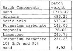
Borosilicate glass compositions for sintering agent, dielectric compositions and multilayer ceramic capacitor using the same
PatentActiveUS20100165542A1
Innovation
- Borosilicate glass compositions are used as a sintering agent, formulated with specific ratios of alkali oxides, alkaline earth oxides, and rare earth oxides, which allow for low-temperature sintering of ceramic dielectrics and enhance hot insulation resistance by forming a stable glass network that reduces the sintering temperature to 1100°C or less.
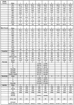
Intermediate thermal expansion coefficient glass
PatentWO2010042460A2
Innovation
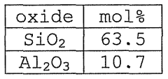
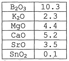
- Developing a glass composition with 60-65% SiO2, 8-12% Al2O3, 7-15% B2O3, and 9-15% RO, where M is an alkali metal and R is an alkaline earth metal, which reduces melting temperatures and thermal expansion coefficient, allowing for lower energy consumption and cost-effective production.
Environmental Impact of Glass-based Electronic Manufacturing
The integration of electronics using borosilicate glass substrates presents both opportunities and challenges in terms of environmental impact. Borosilicate glass, known for its low thermal expansion coefficient and excellent chemical resistance, offers potential advantages over traditional substrate materials in electronic manufacturing.
One of the primary environmental benefits of using borosilicate glass in electronic manufacturing is its recyclability. Unlike many composite materials used in electronics, glass can be recycled indefinitely without loss of quality. This characteristic aligns well with circular economy principles, potentially reducing the overall environmental footprint of electronic devices over their lifecycle.
However, the manufacturing process of borosilicate glass itself requires high temperatures, typically around 1,600°C, which translates to significant energy consumption. This energy-intensive production process contributes to greenhouse gas emissions if not powered by renewable energy sources. Manufacturers adopting this technology must consider strategies to offset these emissions, such as investing in clean energy infrastructure or carbon capture technologies.
The durability of borosilicate glass can lead to longer-lasting electronic components, potentially reducing electronic waste. This is particularly relevant in the context of the growing global e-waste problem. By extending the lifespan of electronic devices, the demand for raw materials and the frequency of device replacement could be reduced, indirectly mitigating environmental impacts associated with resource extraction and waste management.
Water usage in the manufacturing process of glass-based electronics is another environmental consideration. While glass production generally requires less water compared to some semiconductor manufacturing processes, water conservation and recycling strategies should still be implemented to minimize the overall water footprint of the industry.
The chemical resistance of borosilicate glass may also contribute to reduced environmental contamination during the device's use phase and end-of-life disposal. This property could potentially decrease the leaching of harmful substances into the environment, a common concern with electronic waste in landfills.
However, the integration of glass substrates into electronic manufacturing may require new or modified production techniques, potentially involving different chemicals or processes. The environmental impact of these new processes must be carefully assessed and managed to ensure that the benefits of using glass substrates are not outweighed by unforeseen environmental costs in the manufacturing phase.
Thermal Management in Glass-based Integrated Electronics
Thermal management is a critical aspect of integrated electronics using borosilicate glass substrates. As the demand for higher performance and miniaturization in electronic devices continues to grow, effective heat dissipation becomes increasingly challenging. Borosilicate glass, known for its low thermal conductivity, presents unique thermal management considerations in integrated electronics applications.
One of the primary challenges in thermal management for glass-based integrated electronics is the inherent low thermal conductivity of borosilicate glass. This property, while beneficial for certain applications, can lead to heat accumulation in active components, potentially causing performance degradation or device failure. To address this issue, researchers have explored various strategies to enhance heat dissipation in glass-based electronic systems.
A common approach involves the integration of thermal vias or through-glass vias (TGVs) filled with thermally conductive materials. These structures create pathways for heat to flow more efficiently through the glass substrate, significantly improving overall thermal performance. The selection of appropriate filling materials, such as copper or silver, is crucial to maximize heat transfer while maintaining compatibility with the glass substrate.
Another innovative solution is the incorporation of thin-film heat spreaders on the surface of the glass substrate. These heat spreaders, typically made of materials with high thermal conductivity like graphene or diamond-like carbon, help distribute heat more evenly across the substrate surface. This technique is particularly effective in mitigating localized hot spots that can occur in high-power density areas of integrated circuits.
Advanced packaging techniques also play a vital role in thermal management for glass-based integrated electronics. For instance, the use of flip-chip bonding with thermal underfills can enhance heat dissipation from active components to the substrate. Additionally, the development of novel heat sink designs specifically tailored for glass substrates has shown promising results in improving overall thermal performance.
Researchers are also exploring the potential of hybrid substrate materials, combining borosilicate glass with more thermally conductive materials in strategic locations. This approach allows for the retention of glass's desirable properties while addressing its thermal limitations. For example, selective metallization or the integration of high thermal conductivity inserts in critical areas can significantly enhance heat dissipation without compromising the overall benefits of using glass substrates.
As the field of glass-based integrated electronics continues to evolve, thermal simulation and modeling tools are becoming increasingly sophisticated. These tools enable designers to predict and optimize thermal performance early in the development process, leading to more efficient and reliable electronic systems. The integration of such tools with advanced manufacturing techniques is paving the way for innovative thermal management solutions in glass-based electronics.
Unlock deeper insights with PatSnap Eureka Quick Research — get a full tech report to explore trends and direct your research. Try now!
Generate Your Research Report Instantly with AI Agent
Supercharge your innovation with PatSnap Eureka AI Agent Platform!