Resolution and Throughput Tradeoffs in Lithography Algorithms
APR 24, 20269 MIN READ
Generate Your Research Report Instantly with AI Agent
PatSnap Eureka helps you evaluate technical feasibility & market potential.
Lithography Algorithm Development Background and Objectives
Lithography technology has evolved as the cornerstone of semiconductor manufacturing, enabling the continuous miniaturization of electronic devices according to Moore's Law. The fundamental challenge in lithography lies in achieving the precise patterning of increasingly smaller features while maintaining economically viable production speeds. This dual requirement has driven decades of innovation in both hardware systems and computational algorithms.
The historical progression of lithography began with contact and proximity printing methods in the 1960s, advancing through optical projection systems that dominated the industry for several decades. As feature sizes approached the wavelength limits of traditional optical lithography, the industry embraced resolution enhancement techniques including phase-shift masks, optical proximity correction, and immersion lithography. Each advancement required sophisticated algorithmic solutions to manage the complex interactions between light, photoresist, and substrate materials.
Modern lithography algorithms must address the fundamental physics of light diffraction and interference while accounting for manufacturing constraints such as mask complexity, exposure time, and process variations. The transition to extreme ultraviolet lithography and emerging technologies like electron beam lithography has further intensified the computational demands, requiring algorithms that can optimize multiple competing objectives simultaneously.
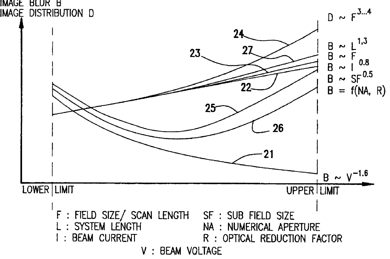
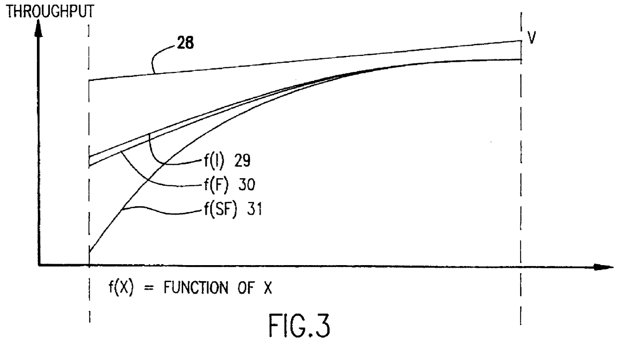
The primary objective of contemporary lithography algorithm development centers on resolving the inherent tension between resolution and throughput. Higher resolution typically demands more complex computational processes, longer exposure times, or multiple patterning steps, all of which reduce manufacturing throughput and increase costs. Conversely, optimizing for throughput often requires compromises in pattern fidelity or limits the achievable minimum feature sizes.
Current research objectives focus on developing intelligent algorithms that can dynamically balance these tradeoffs based on specific design requirements and manufacturing constraints. This includes advancing machine learning approaches for pattern optimization, developing more efficient computational methods for large-scale simulations, and creating adaptive algorithms that can respond to real-time process variations. The ultimate goal is achieving sub-10nm patterning capabilities while maintaining the throughput levels necessary for economically viable mass production in next-generation semiconductor devices.
The historical progression of lithography began with contact and proximity printing methods in the 1960s, advancing through optical projection systems that dominated the industry for several decades. As feature sizes approached the wavelength limits of traditional optical lithography, the industry embraced resolution enhancement techniques including phase-shift masks, optical proximity correction, and immersion lithography. Each advancement required sophisticated algorithmic solutions to manage the complex interactions between light, photoresist, and substrate materials.
Modern lithography algorithms must address the fundamental physics of light diffraction and interference while accounting for manufacturing constraints such as mask complexity, exposure time, and process variations. The transition to extreme ultraviolet lithography and emerging technologies like electron beam lithography has further intensified the computational demands, requiring algorithms that can optimize multiple competing objectives simultaneously.
The primary objective of contemporary lithography algorithm development centers on resolving the inherent tension between resolution and throughput. Higher resolution typically demands more complex computational processes, longer exposure times, or multiple patterning steps, all of which reduce manufacturing throughput and increase costs. Conversely, optimizing for throughput often requires compromises in pattern fidelity or limits the achievable minimum feature sizes.
Current research objectives focus on developing intelligent algorithms that can dynamically balance these tradeoffs based on specific design requirements and manufacturing constraints. This includes advancing machine learning approaches for pattern optimization, developing more efficient computational methods for large-scale simulations, and creating adaptive algorithms that can respond to real-time process variations. The ultimate goal is achieving sub-10nm patterning capabilities while maintaining the throughput levels necessary for economically viable mass production in next-generation semiconductor devices.
Market Demand for High-Resolution Lithography Solutions
The semiconductor industry faces unprecedented demand for advanced lithography solutions as device manufacturers push toward smaller node technologies. The transition to extreme ultraviolet lithography and advanced deep ultraviolet systems has created substantial market opportunities, driven primarily by the need to maintain Moore's Law progression while addressing increasingly complex manufacturing requirements.
Mobile device manufacturers represent the largest segment driving high-resolution lithography demand. The proliferation of smartphones, tablets, and wearable devices requires processors with enhanced performance and energy efficiency, necessitating feature sizes below 7 nanometers. This consumer electronics boom has established sustained demand for cutting-edge lithography equipment capable of achieving sub-wavelength patterning with exceptional precision.
Data center and cloud computing infrastructure expansion significantly amplifies market requirements for advanced lithography solutions. Hyperscale data centers demand processors with superior computational density and reduced power consumption, driving semiconductor manufacturers to adopt the most sophisticated lithography technologies available. The artificial intelligence and machine learning revolution further intensifies these requirements, as specialized chips require intricate circuit patterns achievable only through high-resolution lithography processes.
Automotive industry electrification and autonomous vehicle development create emerging demand segments for specialized semiconductor devices. Advanced driver assistance systems, electric vehicle power management, and autonomous driving processors require robust, high-performance chips manufactured using precise lithography techniques. This automotive semiconductor market expansion represents a growing revenue stream for lithography equipment manufacturers.
Memory manufacturers constitute another critical demand driver, particularly for DRAM and NAND flash production. The exponential growth in data generation and storage requirements across industries necessitates memory devices with higher density and improved performance characteristics. These manufacturing demands require lithography systems capable of producing increasingly complex three-dimensional structures with nanometer-scale precision.
Geopolitical factors and supply chain considerations have intensified regional demand for domestic lithography capabilities. Government initiatives promoting semiconductor manufacturing independence have created substantial investment opportunities in lithography infrastructure, particularly in regions seeking to establish comprehensive semiconductor production ecosystems.
The market exhibits strong growth trajectories across multiple application segments, with particularly robust demand emerging from next-generation computing applications, including quantum computing components and neuromorphic processors. These specialized applications require lithography solutions capable of producing novel device architectures with unprecedented precision requirements, establishing new market niches for advanced lithography technologies.
Current Lithography Algorithm Limitations and Challenges
Current lithography algorithms face fundamental limitations that create an inherent tension between achieving high resolution and maintaining acceptable throughput levels. The primary constraint stems from the physical properties of light diffraction and the computational complexity required to overcome these optical limitations through algorithmic approaches.
Resolution enhancement techniques such as optical proximity correction (OPC) and inverse lithography technology (ILT) demand extensive computational resources to model and compensate for optical effects at nanoscale dimensions. These algorithms must process massive datasets representing complex mask geometries while accounting for photoresist behavior, lens aberrations, and process variations. The computational burden increases exponentially as feature sizes shrink below the wavelength of exposure light, requiring more sophisticated mathematical models and iterative optimization processes.
Throughput limitations arise from the sequential nature of current algorithmic approaches, where each optimization iteration requires substantial processing time. Traditional OPC algorithms rely on rule-based corrections that become increasingly inadequate for advanced nodes, necessitating model-based approaches that consume significantly more computational resources. The transition to curvilinear mask shapes and complex assist features further compounds processing time requirements.
Memory bandwidth constraints represent another critical bottleneck, as lithography algorithms must handle terabyte-scale datasets for full-chip processing. Current hardware architectures struggle to provide sufficient data throughput to feed computational units efficiently, leading to underutilized processing capacity and extended runtime periods.
Algorithmic convergence challenges emerge when pursuing extreme resolution targets, where optimization algorithms may require hundreds of iterations to achieve acceptable solutions. The non-convex nature of lithography optimization problems often leads to local minima, requiring multiple solution attempts and further extending processing times.
Manufacturing constraints impose additional limitations, as algorithms must balance theoretical optical performance with practical considerations such as mask manufacturability and process robustness. These requirements often force algorithmic compromises that limit achievable resolution improvements while still demanding substantial computational resources for verification and validation processes.
Existing Resolution-Throughput Optimization Approaches
01 Optical proximity correction (OPC) algorithms for resolution enhancement
Advanced computational algorithms are employed to correct optical proximity effects in lithography patterns. These algorithms analyze and modify mask patterns to compensate for diffraction and process effects, thereby improving the resolution of printed features. The techniques involve iterative calculations and model-based corrections that predict how light will interact with mask features, enabling more accurate pattern transfer at smaller dimensions.- Optical proximity correction (OPC) algorithms for resolution enhancement: Advanced computational lithography techniques employ optical proximity correction algorithms to compensate for diffraction effects and process variations. These algorithms modify mask patterns by adding sub-resolution assist features, adjusting edge positions, and optimizing feature shapes to improve pattern fidelity and resolution at the wafer level. The methods enable printing of features below the optical diffraction limit while maintaining pattern accuracy.
- Multi-patterning and decomposition techniques: Pattern decomposition methods split complex layouts into multiple simpler masks that are sequentially exposed and processed. These techniques include double patterning, triple patterning, and self-aligned multiple patterning approaches. Decomposition algorithms optimize the assignment of features to different masks while minimizing conflicts and maintaining design intent, enabling higher resolution beyond single-exposure limitations.
- Source-mask optimization (SMO) for throughput improvement: Simultaneous optimization of illumination source patterns and mask designs maximizes imaging performance while considering manufacturing constraints. These algorithms balance resolution enhancement with exposure dose requirements and depth of focus. The co-optimization approach enables faster convergence to optimal solutions and can significantly improve wafer throughput by reducing required exposure doses while maintaining pattern quality.
- Machine learning and inverse lithography techniques: Computational methods employ inverse problem solving and machine learning algorithms to directly calculate optimal mask patterns from desired wafer patterns. These approaches use iterative optimization, neural networks, or other artificial intelligence techniques to accelerate the design process and improve solution quality. The methods can handle complex design rules and manufacturing constraints while reducing computation time compared to traditional rule-based approaches.
- Fast simulation and modeling algorithms: Efficient computational models simulate lithographic imaging processes with reduced complexity while maintaining accuracy. These include compact models, lookup table approaches, and hierarchical simulation methods that exploit pattern regularity. Acceleration techniques such as parallel processing, GPU computing, and adaptive sampling enable rapid verification of large-scale designs, improving overall throughput in the mask design and verification workflow.
02 Multi-patterning and decomposition techniques
Pattern decomposition methods split complex layouts into multiple simpler patterns that are exposed sequentially. This approach overcomes single-exposure resolution limitations by using multiple lithography steps with different masks. The decomposition algorithms optimize how patterns are divided to minimize conflicts and maximize manufacturing yield while achieving higher effective resolution than single-patterning approaches.Expand Specific Solutions03 Source-mask optimization (SMO) for enhanced imaging
Simultaneous optimization of illumination source shapes and mask patterns improves lithographic imaging performance. These algorithms co-optimize both the light source configuration and mask design to maximize process windows and resolution. The computational methods balance multiple objectives including contrast, depth of focus, and pattern fidelity to achieve optimal imaging conditions for critical features.Expand Specific Solutions04 Throughput optimization through parallel processing and computational efficiency
Advanced computational architectures and algorithms accelerate lithography calculations to increase manufacturing throughput. These methods employ parallel processing, hierarchical data structures, and optimized algorithms to reduce computation time for mask correction and verification. The techniques enable faster turnaround times for mask preparation while maintaining accuracy, directly impacting wafer production rates.Expand Specific Solutions05 Machine learning and AI-based lithography optimization
Artificial intelligence and machine learning techniques are applied to lithography process optimization and prediction. These approaches use trained models to rapidly predict lithographic outcomes, optimize process parameters, and correct patterns. The methods can learn from historical data to improve accuracy and speed compared to traditional physics-based simulations, enabling both better resolution and higher throughput through faster convergence.Expand Specific Solutions
Key Players in Lithography Software and EDA Industry
The lithography algorithms sector addressing resolution and throughput tradeoffs represents a mature yet rapidly evolving industry driven by semiconductor scaling demands. The market demonstrates substantial scale, with global lithography equipment revenues exceeding $20 billion annually, primarily concentrated among established players. Technology maturity varies significantly across the competitive landscape. ASML Netherlands BV dominates extreme ultraviolet (EUV) lithography with the most advanced solutions, while Applied Materials and Tokyo Electron provide complementary process equipment. Leading foundries including TSMC, GlobalFoundries, and SMIC drive algorithm optimization requirements through their advanced node manufacturing. Memory manufacturers like SK Hynix and Micron Technology push specialized patterning solutions. Research institutions such as EPFL and Beijing Institute of Technology contribute fundamental algorithm innovations, while companies like Siemens Industry Software develop computational lithography tools. The industry exhibits high barriers to entry due to substantial R&D investments and complex integration requirements, creating a concentrated competitive structure with established technology leaders maintaining significant advantages.
ASML Netherlands BV
Technical Solution: ASML has developed advanced computational lithography algorithms that optimize the tradeoff between resolution and throughput in extreme ultraviolet (EUV) lithography systems. Their approach utilizes sophisticated optical proximity correction (OPC) and source mask optimization (SMO) techniques to achieve sub-7nm resolution while maintaining acceptable wafer throughput rates. The company's NXE series EUV scanners incorporate real-time dose control algorithms and advanced metrology feedback systems to balance pattern fidelity with production efficiency. Their computational lithography suite includes machine learning-enhanced algorithms that predict and compensate for systematic variations, enabling high-resolution patterning at commercially viable throughput levels for advanced semiconductor manufacturing.
Strengths: Industry-leading EUV technology with superior resolution capabilities and comprehensive computational lithography solutions. Weaknesses: High system complexity and cost, requiring significant infrastructure investment and specialized expertise.
Applied Materials, Inc.
Technical Solution: Applied Materials has developed integrated lithography solutions that address resolution-throughput tradeoffs through their advanced patterning and process control technologies. Their approach combines computational lithography algorithms with materials engineering and process optimization to enhance pattern fidelity while maintaining production efficiency. The company's Centura platform incorporates real-time process monitoring and adaptive control algorithms that dynamically adjust exposure parameters based on wafer-level variations. Their lithography enhancement technologies include advanced resist processing, etch selectivity optimization, and multi-patterning techniques that enable high-resolution features without significantly compromising throughput in high-volume manufacturing environments.
Strengths: Comprehensive materials and process expertise with integrated solutions for advanced patterning challenges. Weaknesses: Dependent on partnerships for lithography equipment, requiring coordination across multiple technology platforms.
Core Algorithms for Resolution-Throughput Balance
Cluster e-beam lithography system
PatentInactiveUS20090121159A1
Innovation
- A hybrid system combining optical and cluster e-beam lithography, where optical lithography exposes larger patterns and cluster e-beam lithography handles smaller features, with a control center managing wafer processing and data flow to enhance throughput.


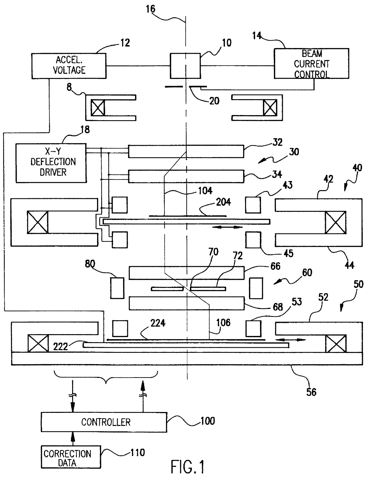
Electron beam projection lithography system (EBPS)
PatentInactiveUS6069684A
Innovation
- An electron beam projection system with specific configurations and operating parameters, including a deflection arrangement for orthogonal scanning, a beam current of 4-35 μA, beam energy of 75-175 kV, sub-field size of 0.1-0.5 mm, and numerical aperture of 3-8 mrad, optimized for dual-scanning modes and continuous motion of the reticle and wafer, to achieve high resolution and throughput.
Semiconductor Manufacturing Standards and Regulations
The semiconductor manufacturing industry operates under a comprehensive framework of standards and regulations that directly impact lithography algorithm development and implementation. International standards organizations such as SEMI (Semiconductor Equipment and Materials International), ISO (International Organization for Standardization), and JEDEC (Joint Electron Device Engineering Council) establish critical guidelines for lithographic processes, equipment specifications, and quality control measures. These standards define acceptable parameters for resolution accuracy, overlay precision, and throughput metrics that lithography algorithms must achieve to ensure manufacturing compliance.
Regulatory compliance in semiconductor fabrication facilities requires adherence to strict environmental, safety, and quality standards that influence algorithm design choices. The FDA's regulations for medical device semiconductors, automotive industry standards like ISO 26262 for safety-critical applications, and aerospace standards such as AS9100 impose additional constraints on lithographic processes. These regulations often mandate specific traceability requirements, statistical process control measures, and validation protocols that affect how resolution and throughput optimization algorithms are implemented and documented.
Quality management systems, particularly ISO 9001 and industry-specific standards like IATF 16949, establish mandatory documentation and validation procedures for lithographic processes. These requirements influence algorithm development by necessitating comprehensive testing protocols, statistical validation of performance metrics, and detailed record-keeping of process parameters. The standards mandate that any algorithmic modifications affecting resolution or throughput must undergo rigorous qualification procedures, including capability studies and long-term stability assessments.
Export control regulations, including the Export Administration Regulations (EAR) and International Traffic in Arms Regulations (ITAR), significantly impact the development and deployment of advanced lithography algorithms. These regulations restrict the transfer of cutting-edge lithographic technologies and algorithms to certain countries, influencing how companies approach algorithm optimization and technology sharing. Compliance requirements often necessitate additional security measures and documentation protocols that can affect algorithm implementation timelines and collaborative research efforts.
Environmental regulations such as REACH (Registration, Evaluation, Authorization and Restriction of Chemicals) and RoHS (Restriction of Hazardous Substances) indirectly influence lithography algorithm development by constraining the materials and processes that can be utilized. These regulations may limit certain optimization approaches or require alternative algorithmic strategies to achieve desired resolution and throughput targets while maintaining environmental compliance, thereby shaping the technical landscape within which algorithm developers must operate.
Cost-Performance Analysis in Lithography Processing
The cost-performance dynamics in lithography processing represent a critical balancing act between achieving desired resolution capabilities and maintaining economically viable throughput levels. Modern semiconductor manufacturing facilities face mounting pressure to optimize this relationship as device geometries continue to shrink while production volumes increase. The fundamental challenge lies in the inverse relationship between resolution enhancement and processing speed, where higher precision typically demands longer exposure times and more complex processing steps.
Capital expenditure considerations dominate the cost structure of advanced lithography systems. Extreme ultraviolet (EUV) lithography tools, while offering superior resolution capabilities, require investments exceeding $200 million per unit. These systems demonstrate significantly lower throughput compared to deep ultraviolet (DUV) alternatives, processing approximately 140-170 wafers per hour versus 275-300 wafers per hour for mature ArF immersion systems. The cost per wafer processed becomes a crucial metric, incorporating not only equipment depreciation but also operational expenses including maintenance, consumables, and facility requirements.
Operational cost analysis reveals substantial differences across lithography technologies. EUV systems consume considerably more power, typically requiring 1-1.5 MW compared to 0.3-0.5 MW for DUV systems. Additionally, EUV processing demands specialized infrastructure including hydrogen gas supply systems, contamination control mechanisms, and enhanced clean room specifications. These requirements translate to elevated operational costs that must be weighed against the performance benefits of improved resolution and reduced process complexity.
The economic impact of yield considerations significantly influences cost-performance calculations. Higher resolution lithography systems often demonstrate improved pattern fidelity and reduced defect rates, leading to enhanced manufacturing yields. This yield improvement can offset higher processing costs, particularly for advanced node production where defect-related losses carry substantial financial implications. The relationship between lithography precision and final product yield becomes increasingly critical as device complexity increases.
Multi-patterning strategies introduce additional cost complexity while addressing resolution limitations of existing systems. Double and quadruple patterning techniques enable advanced node production using mature DUV technology but require multiple exposure steps, increasing both processing time and material consumption. The cost analysis must account for additional mask sets, alignment precision requirements, and overlay control systems necessary for successful multi-patterning implementation.
Performance optimization strategies focus on maximizing throughput while maintaining resolution requirements. Advanced dose control algorithms, improved resist formulations, and enhanced optical proximity correction techniques contribute to processing efficiency gains. These technological improvements help bridge the cost-performance gap by enabling faster processing speeds without compromising pattern quality or dimensional accuracy.
Unlock deeper insights with PatSnap Eureka Quick Research — get a full tech report to explore trends and direct your research. Try now!
Generate Your Research Report Instantly with AI Agent
Supercharge your innovation with PatSnap Eureka AI Agent Platform!