

Validate Dimensions in Computational Lithography Using Simulation Models
APR 24, 20269 MIN READ
Generate Your Research Report Instantly with AI Agent
PatSnap Eureka helps you evaluate technical feasibility & market potential.
Computational Lithography Background and Validation Goals
Computational lithography has emerged as a critical technology in semiconductor manufacturing, representing the convergence of advanced optical physics, mathematical modeling, and computational algorithms to enable precise pattern transfer onto silicon wafers. This field encompasses sophisticated techniques including optical proximity correction (OPC), inverse lithography technology (ILT), and source mask optimization (SMO), which collectively address the fundamental challenges of printing nanoscale features using wavelengths significantly larger than the target dimensions.
The evolution of computational lithography traces back to the early 1990s when feature sizes began approaching the diffraction limits of available light sources. As Moore's Law continued driving dimensional scaling, traditional lithographic approaches became insufficient, necessitating computational interventions to maintain manufacturing feasibility. The transition from 248nm to 193nm lithography, followed by the introduction of immersion lithography and multiple patterning techniques, has been fundamentally enabled by increasingly sophisticated computational models and correction algorithms.
Modern computational lithography systems integrate complex physical models that account for electromagnetic field propagation, photoresist chemistry, and process variations. These models must accurately predict how mask patterns will transfer through the optical system and photoresist stack, considering factors such as polarization effects, lens aberrations, and three-dimensional mask topography. The computational intensity has grown exponentially, with current full-chip OPC requiring massive parallel processing capabilities and advanced algorithmic optimization.
The primary technical objectives in computational lithography validation center on achieving dimensional accuracy within increasingly tight tolerances while maintaining acceptable computational throughput. Critical dimension (CD) control requirements have tightened to sub-nanometer precision for advanced nodes, demanding validation methodologies that can verify model accuracy across diverse pattern geometries, pitch conditions, and process windows. Edge placement error (EPE) has become the fundamental metric, requiring comprehensive validation across millions of measurement points.
Validation goals extend beyond static dimensional accuracy to encompass process robustness and manufacturability. Models must demonstrate predictive capability across focus and exposure variations, mask manufacturing tolerances, and systematic process drifts. The validation framework must establish confidence in model predictions for both isolated and dense pattern environments, considering proximity effects, loading dependencies, and through-pitch behavior that directly impact yield and device performance in production environments.
Market Demand for Advanced Lithography Simulation
The semiconductor industry's relentless pursuit of smaller node technologies has created an unprecedented demand for advanced lithography simulation solutions. As chip manufacturers push toward 3nm, 2nm, and beyond, the complexity of photolithography processes has reached levels where traditional trial-and-error approaches become economically prohibitive. The need for accurate dimensional validation through computational models has transformed from a convenience to an absolute necessity for maintaining competitive advantage and ensuring manufacturing viability.
Market drivers for advanced lithography simulation are primarily fueled by the exponential increase in mask costs and the shrinking process windows at advanced nodes. Leading foundries and integrated device manufacturers face mounting pressure to achieve first-pass success in their lithography processes, as each iteration can cost millions of dollars and months of development time. The ability to predict and validate critical dimensions before committing to expensive mask sets has become a critical capability that directly impacts time-to-market and profitability.
The emergence of extreme ultraviolet lithography has further intensified the demand for sophisticated simulation tools. EUV processes introduce unique challenges including stochastic effects, mask 3D effects, and complex resist chemistry interactions that cannot be adequately addressed through conventional modeling approaches. This has created a specialized market segment for EUV-specific simulation solutions that can accurately predict dimensional variations and process sensitivities.
Memory manufacturers represent a particularly strong demand segment, driven by their need for precise control over critical dimensions in high-density storage devices. The transition to 3D NAND architectures and advanced DRAM structures requires simulation tools capable of modeling complex multi-layer interactions and aspect ratio dependent etching effects. These applications demand not only accuracy but also computational efficiency to handle the massive datasets involved in memory device optimization.
The artificial intelligence and machine learning revolution has created additional market opportunities for simulation vendors. Modern lithography simulation platforms increasingly incorporate AI-driven optimization algorithms and predictive analytics capabilities, enabling more sophisticated process control and yield enhancement strategies. This convergence of traditional physics-based modeling with advanced data analytics has opened new revenue streams and expanded the addressable market significantly.
Emerging applications in automotive semiconductors, 5G infrastructure, and edge computing devices are driving demand for specialized simulation capabilities tailored to these specific market requirements. Each application domain presents unique challenges in terms of device geometries, performance specifications, and reliability requirements, creating opportunities for targeted simulation solutions that address these specialized needs.
Current State of Dimensional Validation in Lithography
Dimensional validation in computational lithography has evolved significantly over the past decade, driven by the relentless push toward smaller feature sizes and increased pattern complexity in semiconductor manufacturing. Current validation methodologies primarily rely on a combination of optical proximity correction (OPC) models, process variation models, and metrology-based verification systems to ensure dimensional accuracy across various lithographic processes.
The industry standard approach involves multi-stage validation workflows that integrate resist models, optical models, and etch models to predict final feature dimensions. Leading semiconductor manufacturers typically employ rigorous calibration procedures using scanning electron microscopy (SEM) measurements and critical dimension (CD) data from production wafers. These calibration datasets serve as ground truth for model accuracy assessment, with typical validation requirements demanding dimensional prediction errors within 1-2 nanometers for critical features.
Advanced computational frameworks now incorporate machine learning algorithms to enhance model predictive capabilities, particularly for complex three-dimensional structures and non-rectangular geometries. Process window modeling has become increasingly sophisticated, enabling validation across multiple exposure conditions, focus variations, and dose fluctuations simultaneously. This comprehensive approach addresses the inherent variability in modern lithographic processes while maintaining acceptable computational efficiency.
Current validation protocols face significant challenges in addressing emerging lithographic techniques such as extreme ultraviolet (EUV) lithography and directed self-assembly (DSA). Traditional validation approaches struggle with the stochastic effects prevalent in EUV processes, where photon shot noise and resist line edge roughness create dimensional variations that are difficult to model accurately. Additionally, the increasing adoption of multi-patterning techniques requires validation methodologies that can handle complex overlay dependencies and cumulative dimensional errors across multiple exposure steps.
The integration of artificial intelligence and deep learning techniques represents a growing trend in dimensional validation, with several major foundries developing neural network-based models that can capture non-linear relationships between process parameters and final dimensions. These AI-enhanced validation systems demonstrate improved accuracy for complex pattern interactions and edge cases that traditional physics-based models struggle to predict reliably.
Despite these advances, current validation methodologies still exhibit limitations in handling full-chip complexity and cross-field dimensional variations, necessitating continued research into more robust and scalable validation approaches for next-generation lithographic processes.
Existing Dimensional Validation Solutions
01 Optical Proximity Correction (OPC) techniques for sub-wavelength lithography
Computational lithography employs optical proximity correction methods to compensate for diffraction effects that occur when feature sizes approach or fall below the wavelength of light used in photolithography. These techniques involve modifying mask patterns through model-based calculations to predict and correct how light will interact with photoresist, ensuring that printed features match intended dimensions. Advanced algorithms analyze the optical behavior and apply corrections such as serif additions, line biasing, and assist features to achieve accurate pattern transfer at nanometer scales.- Optical Proximity Correction (OPC) techniques for sub-wavelength lithography: Computational lithography methods employ optical proximity correction to compensate for diffraction effects in sub-wavelength feature printing. These techniques use model-based approaches to predict and correct pattern distortions that occur during the lithography process. Advanced algorithms analyze target patterns and generate corrected mask layouts that account for optical interference effects, enabling accurate reproduction of features smaller than the exposure wavelength. The correction process involves iterative simulations and adjustments to optimize the final printed patterns on wafers.
- Source-mask optimization (SMO) for enhanced pattern fidelity: Source-mask optimization represents an integrated approach to computational lithography where both the illumination source and mask patterns are co-optimized simultaneously. This technique extends beyond traditional mask-only optimization by adjusting the spatial and angular distribution of illumination to maximize imaging performance. The optimization process considers the coupled effects of source shape, mask transmission, and target pattern requirements to achieve improved process windows and pattern fidelity. This approach is particularly effective for complex two-dimensional patterns and critical layers in advanced semiconductor manufacturing.
- Machine learning and inverse lithography technology: Advanced computational methods utilize machine learning algorithms and inverse lithography techniques to solve complex mask synthesis problems. These approaches work backwards from desired wafer patterns to determine optimal mask configurations, often producing non-intuitive mask shapes that achieve superior printing results. Neural networks and deep learning models can be trained on large datasets of lithography simulations to accelerate the optimization process and predict optimal solutions. The integration of artificial intelligence enables faster convergence and handling of increasingly complex design rules in advanced technology nodes.
- Multi-patterning decomposition and coloring algorithms: Computational techniques for multi-patterning lithography involve decomposing dense layout patterns into multiple mask layers that can be printed separately and combined on the wafer. These algorithms solve complex graph coloring and pattern assignment problems to minimize conflicts while maintaining design intent. The decomposition process must consider manufacturing constraints, overlay tolerances, and stitching requirements between different exposure passes. Advanced methods incorporate awareness of process variations and optimize the decomposition to maximize yield and minimize edge placement errors.
- Process window optimization and lithography hotspot detection: Computational lithography includes methods for analyzing and optimizing the process window to ensure robust manufacturing across variations in focus, dose, and other process parameters. Hotspot detection algorithms identify layout patterns that are susceptible to printing failures or yield loss under process variations. These techniques employ fast pattern matching, machine learning classification, and full-chip simulation to screen designs for potential lithography issues. The optimization process adjusts mask patterns and process conditions to maximize the overlap of acceptable process windows across all critical features, ensuring manufacturability at high volumes.
02 Source-Mask Optimization (SMO) for enhanced resolution
Source-mask optimization represents an integrated approach where both the illumination source configuration and mask design are simultaneously optimized to maximize lithographic performance. This computational method explores the design space of pupil illumination patterns and mask geometries together, enabling better control over imaging characteristics and extending the resolution capabilities of existing lithography equipment. The optimization process typically involves iterative algorithms that balance multiple objectives including pattern fidelity, process window, and manufacturing constraints.Expand Specific Solutions03 Inverse Lithography Technology (ILT) for mask synthesis
Inverse lithography technology approaches mask design from a fundamentally different perspective by starting with the desired wafer pattern and working backwards to determine the optimal mask pattern. This computational approach treats mask synthesis as an inverse problem, using sophisticated mathematical optimization to generate mask patterns that may appear counter-intuitive but produce superior wafer results. The methodology enables the creation of complex curvilinear mask shapes and continuous tone variations that maximize process margins and pattern fidelity beyond what rule-based approaches can achieve.Expand Specific Solutions04 Machine learning and AI-based lithography modeling
Modern computational lithography increasingly incorporates machine learning algorithms and artificial intelligence techniques to accelerate simulation processes and improve prediction accuracy. These methods train neural networks or other learning models on extensive datasets of lithographic simulations and measurements to create fast surrogate models that can predict lithographic outcomes. The approach significantly reduces computational time while maintaining accuracy, enabling rapid design iterations and real-time optimization during mask design and manufacturing processes.Expand Specific Solutions05 Multi-patterning decomposition and computational solutions
As feature dimensions continue to shrink beyond single-exposure capabilities, multi-patterning techniques require sophisticated computational algorithms to decompose complex layouts into multiple mask layers. These computational methods solve graph-coloring and pattern assignment problems while considering manufacturing constraints, overlay tolerances, and design rule requirements. Advanced algorithms optimize the decomposition to minimize conflicts, reduce the number of stitches, and ensure manufacturability across multiple exposure steps, enabling the production of features at dimensions well below the optical resolution limit.Expand Specific Solutions
Key Players in Lithography Simulation Industry
The computational lithography dimension validation market represents a mature yet rapidly evolving sector within the semiconductor manufacturing ecosystem. Currently valued at several billion dollars globally, this market is experiencing significant growth driven by the industry's transition to advanced process nodes below 7nm and the increasing complexity of chip designs. The technology maturity varies considerably across different solution providers, with established leaders like ASML Netherlands BV and Taiwan Semiconductor Manufacturing Co. Ltd. demonstrating highly mature EUV lithography and foundry capabilities, while EDA giants Synopsys Inc. and Cadence Design Systems Inc. offer sophisticated simulation platforms. Emerging players such as Dongfang Jingyuan Electron Ltd. and D2S Inc. are developing specialized solutions for yield management and e-beam lithography respectively. Major foundries including Samsung Electronics, GLOBALFOUNDRIES, and Chinese manufacturers like SMIC are actively implementing advanced computational lithography techniques, while research institutions like Fraunhofer-Gesellschaft and Interuniversitair Micro-Electronica Centrum continue pushing technological boundaries, indicating a competitive landscape characterized by both established dominance and innovative disruption.
ASML Netherlands BV
Technical Solution: ASML develops advanced computational lithography solutions integrated with their EUV and DUV lithography systems. Their simulation models incorporate sophisticated optical proximity correction (OPC) and source mask optimization (SMO) algorithms to validate critical dimensions before actual wafer exposure. The company's Brion division provides comprehensive computational lithography software that enables accurate prediction of on-wafer CD performance through rigorous electromagnetic field simulations and process modeling. Their solutions integrate machine learning algorithms to enhance model accuracy and reduce computational time while maintaining precision for advanced node manufacturing below 7nm.
Strengths: Market leader in lithography equipment with deep integration between hardware and software, extensive process knowledge. Weaknesses: High cost of solutions, complex implementation requiring specialized expertise.
Cadence Design Systems, Inc.
Technical Solution: Cadence offers the Litho Physical Analyzer (LPA) and Cerebrus Intelligent Chip Explorer for computational lithography validation. Their platform combines rigorous lithography simulation with machine learning-enhanced models to predict and validate critical dimensions across full-chip layouts. The solution includes advanced OPC verification, hotspot detection, and process window analysis capabilities. Cadence integrates lithography-aware design optimization throughout the design flow, enabling early detection of manufacturability issues and providing feedback for design rule optimization and mask synthesis.
Strengths: Comprehensive EDA ecosystem integration, strong machine learning capabilities, full-chip analysis. Weaknesses: Requires significant computational resources, steep learning curve for complex features.
Core Innovations in Lithography Simulation Models
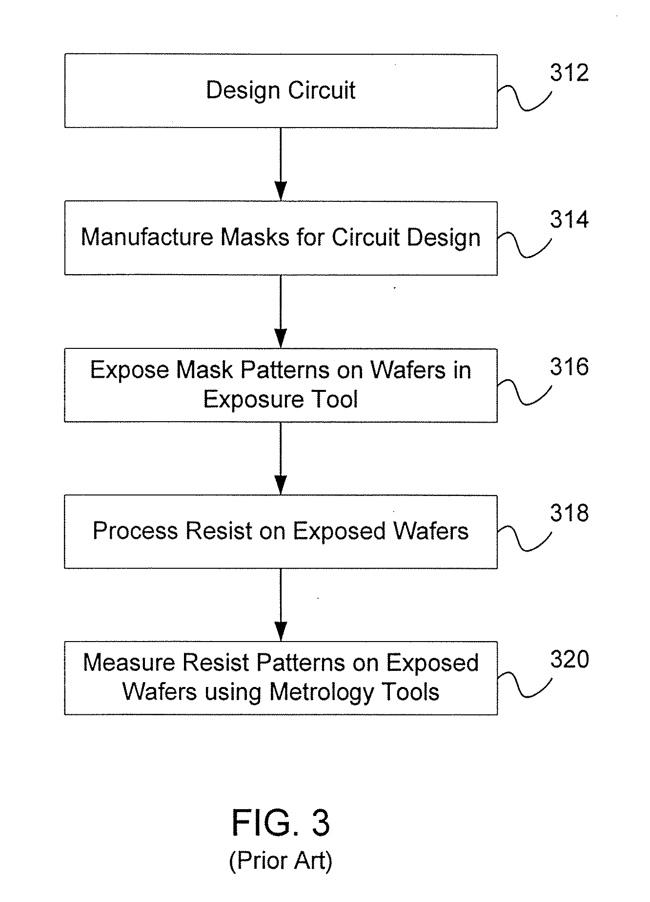
Calibration of lithographic process models
PatentInactiveUS20100171031A1
Innovation
- A method that involves providing a lithographic process model with calibration patterns, determining bin values for image parameters, transferring these patterns to form printed images, and evaluating the parameter space coverage to ensure adequate population, with modifications made to the calibration patterns as needed to achieve complete coverage.


Method for lithography model calibration
PatentActiveUS20070032896A1
Innovation
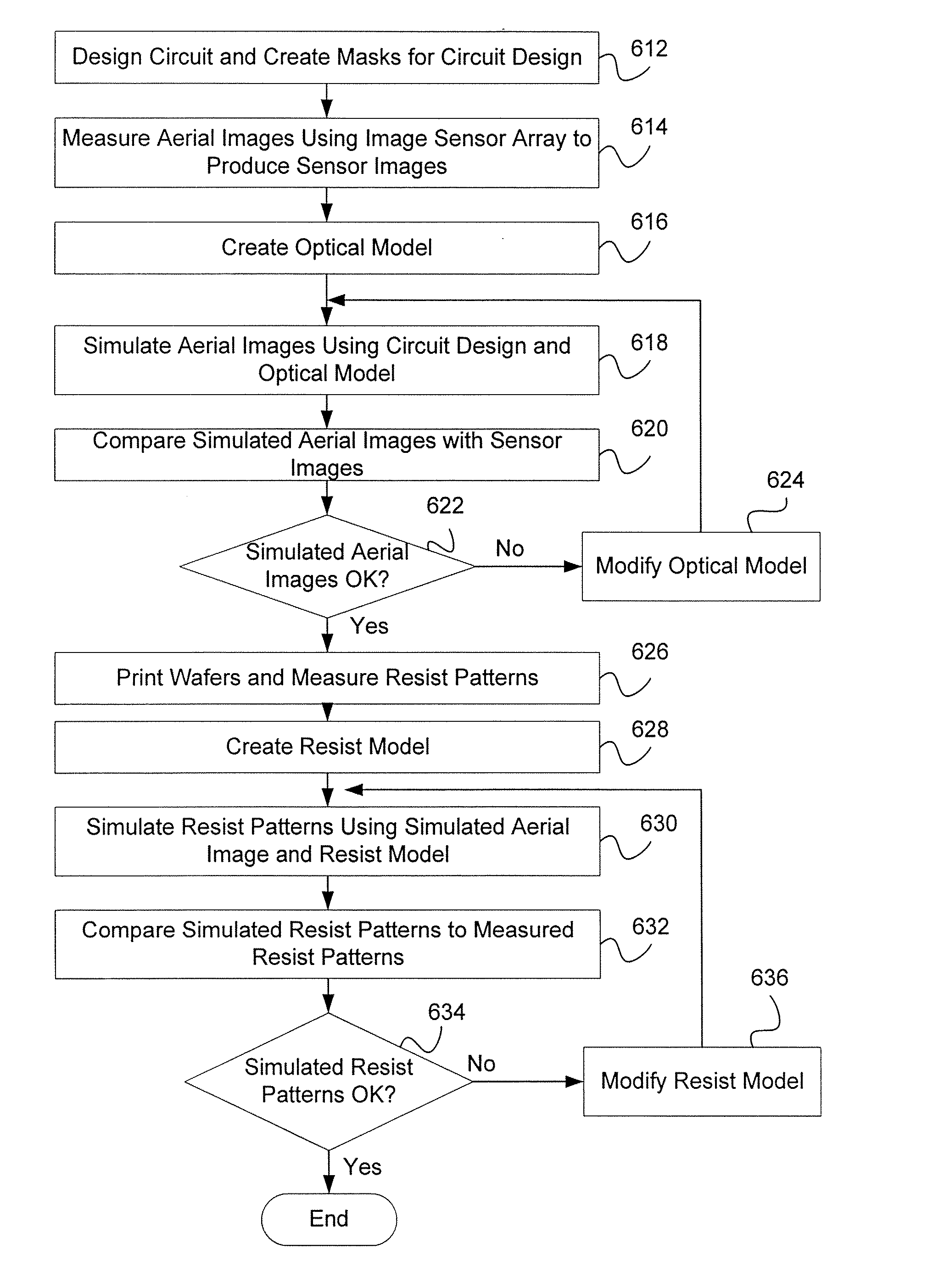
- A method that uses in-situ aerial image measurements from an image sensor array to separately calibrate optical and resist models, improving the accuracy and separability of these components, allowing for better pattern transfer prediction and model-based process control.

Semiconductor Manufacturing Standards and Regulations
The semiconductor manufacturing industry operates under a comprehensive framework of standards and regulations that directly impact computational lithography validation processes. International standards organizations such as SEMI, IEEE, and ISO have established critical guidelines for dimensional measurement and validation methodologies in semiconductor fabrication. These standards define acceptable tolerances, measurement protocols, and quality assurance procedures that simulation models must adhere to when validating lithographic dimensions.
SEMI standards, particularly those in the E10 series, establish fundamental requirements for equipment performance and process control in semiconductor manufacturing. These specifications mandate specific accuracy levels for dimensional measurements, typically requiring sub-nanometer precision in critical dimension control. The standards also define statistical process control methods that must be integrated into simulation validation workflows, ensuring that computational models meet industry-accepted reliability criteria.
Regulatory compliance extends beyond technical specifications to encompass environmental and safety considerations. The European Union's RoHS directive and REACH regulations impose restrictions on materials used in semiconductor manufacturing, which directly affects the chemical processes modeled in computational lithography simulations. Similarly, export control regulations such as the Wassenaar Arrangement influence the development and distribution of advanced lithography simulation technologies.
Quality management systems based on ISO 9001 and automotive-specific standards like ISO/TS 16949 require comprehensive documentation and traceability of validation processes. This necessitates that simulation models incorporate audit trails and validation records that demonstrate compliance with dimensional accuracy requirements. The standards mandate regular calibration of measurement systems and validation of computational models against certified reference materials.
Regional regulatory variations present additional complexity for global semiconductor manufacturers. The United States' NIST guidelines differ from European EURAMET standards in certain measurement methodologies, requiring simulation models to accommodate multiple validation frameworks. Asian markets, particularly Japan and South Korea, have developed their own complementary standards that emphasize specific aspects of dimensional control relevant to their manufacturing ecosystems.
Emerging regulations addressing cybersecurity and intellectual property protection are increasingly relevant to computational lithography validation. Standards such as IEC 62443 for industrial cybersecurity require secure implementation of simulation models and protection of proprietary dimensional data throughout the validation process.
Process Control Integration in Lithography Systems
Process control integration in lithography systems represents a critical advancement in semiconductor manufacturing, where real-time monitoring and feedback mechanisms are seamlessly incorporated into the lithography workflow. This integration enables continuous optimization of exposure parameters, overlay accuracy, and critical dimension control throughout the production process.
Modern lithography systems employ sophisticated sensor networks that continuously monitor key process variables including temperature, pressure, vibration, and optical alignment. These sensors feed data into centralized control systems that can make instantaneous adjustments to maintain optimal printing conditions. The integration extends beyond hardware to encompass software algorithms that predict and compensate for systematic variations before they impact product quality.
Advanced process control architectures utilize machine learning algorithms to analyze historical process data and identify patterns that correlate with dimensional variations. These predictive models enable proactive adjustments to exposure dose, focus settings, and reticle positioning based on real-time process conditions and upstream manufacturing data.
The integration framework incorporates multiple feedback loops operating at different time scales. Fast feedback systems respond to immediate process disturbances within milliseconds, while slower adaptive control mechanisms adjust for long-term drift and systematic variations over hours or days. This multi-layered approach ensures both short-term stability and long-term process optimization.
Communication protocols between lithography tools and fab-wide manufacturing execution systems enable coordinated process control across multiple process steps. This holistic integration allows for feed-forward control strategies where measurements from previous process steps inform lithography parameter adjustments, significantly improving overall process capability and yield performance in high-volume manufacturing environments.
Unlock deeper insights with PatSnap Eureka Quick Research — get a full tech report to explore trends and direct your research. Try now!
Generate Your Research Report Instantly with AI Agent
Supercharge your innovation with PatSnap Eureka AI Agent Platform!