
Semiconductor structures and methods of manufacturing and operating the same
A method of operation, semiconductor technology, applied in semiconductor/solid-state device manufacturing, semiconductor devices, electric solid-state devices, etc., can solve the problems of reduced electronic storage space, reduced reliability of storage units, etc.
- Summary
- Abstract
- Description
- Claims
- Application Information
AI Technical Summary
Problems solved by technology
Method used
Image

Examples
Embodiment Construction
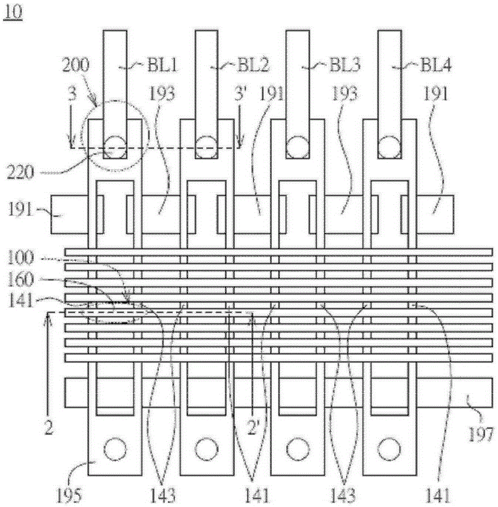
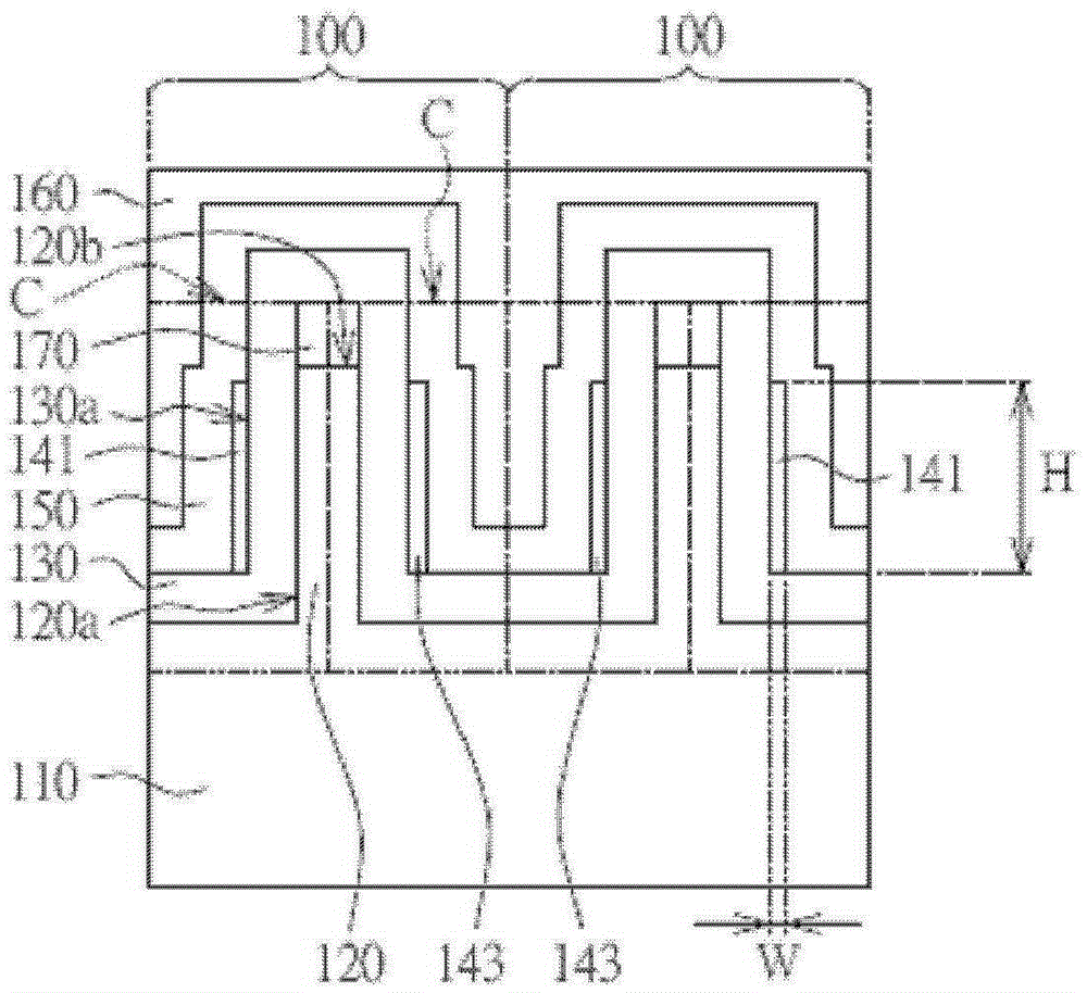
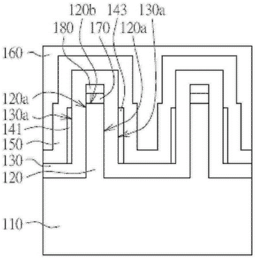
[0052] In the embodiments of the present invention, a semiconductor structure and its manufacturing method and operation method are proposed. The first strip-shaped conductive block and the second strip-shaped conductive block of the semiconductor structure are respectively formed on the two side walls of a main structure, which can effectively increase the memory storage capacity per unit area in the horizontal direction, and maintain sufficient memory storage capacity to be effective The size miniaturization of the storage device is achieved, and the operation control and operation reliability of the storage device are improved. However, the detailed structures, process steps and operation steps proposed in the embodiments are for illustration purposes only, and are not intended to limit the protection scope of the present invention. The various steps are for illustration only, and are not intended to limit the present invention. Those with ordinary knowledge can modify or ...
PUM
 Abstract
Description
Claims
Application Information