
Display panel, manufacturing method thereof, and display device
A technology for display panels and display substrates, which is applied in the manufacturing of semiconductor/solid-state devices, semiconductor devices, electrical components, etc., can solve the problems of uneven film formation and complex thin-film packaging processes, avoid window effects, reduce production costs, and reduce The effect of complexity
Patent Information
- Authority / Receiving Office
- CN · China
- Patent Type
- Patents(China)
- Current Assignee / Owner
- Publication Date
- 2020-04-03
Smart Images
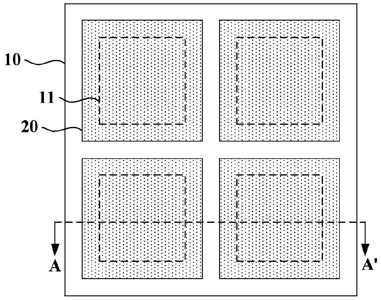
Figure 1 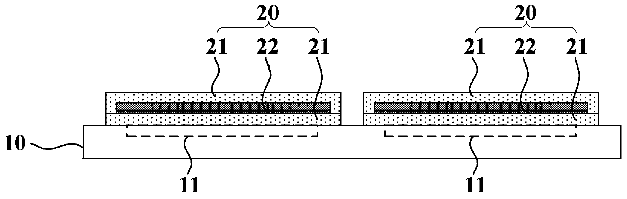
Figure 2 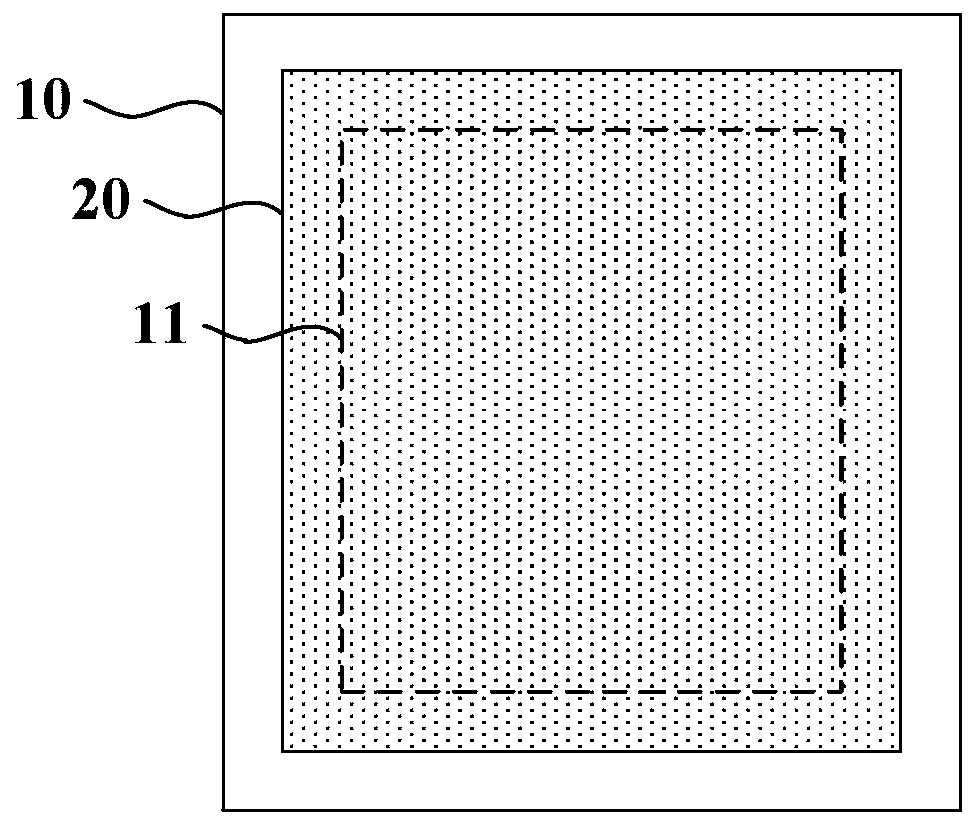
Figure 3
Abstract
Description
technical field
[0001] Embodiments of the present invention relate to display technologies, and in particular to a display panel, a manufacturing method thereof, and a display device. Background technique
[0002] With the development of display technology, the application of flexible display technology is becoming more and more extensive. The existing flexible organic light emitting display panel structure generally includes a flexible substrate, a display device layer, and a thin film encapsulation layer. The thin film encapsulation layer generally includes an inorganic layer and an organic layer, the inorganic layer is used to block water and oxygen, and the organic layer is used to improve the flexibility of the thin film encapsulation layer.
[0003] In a flexible organic light-emitting display panel, the inorganic layer of the thin film encapsulation layer is usually deposited after alignment using a mask mask. Specifically, before forming the thin film encapsulation...
Examples
Embodiment Construction
[0032] In order to make the purpose, technical solutions and advantages of the present invention clearer, the technical solutions of the present invention will be clearly and completely described through implementation with reference to the accompanying drawings in the embodiments of the present invention. Obviously, the described embodiments are the embodiment of the present invention. Some, but not all, embodiments. Based on the embodiments of the present invention, all other embodiments obtained by persons of ordinary skill in the art without making creative efforts belong to the protection scope of the present invention.
[0033] refer to figure 1 As shown in , it is a schematic diagram of a display panel provided by an embodiment of the present invention. The display panel provided in this embodiment includes: a display substrate 10, the display substrate 10 includes at least one display area 11; an encapsulation structure 20 encapsulating the display area 11, the encaps...