
Manufacturing method of array substrate, array substrate and display device
The technology of an array substrate and a manufacturing method, which is applied in the field of array substrates and display devices, can solve problems such as uneven light emission of light-emitting diode display devices
Patent Information
- Authority / Receiving Office
- CN · China
- Patent Type
- Applications(China)
- Current Assignee / Owner
- Publication Date
- 2019-07-09
Smart Images
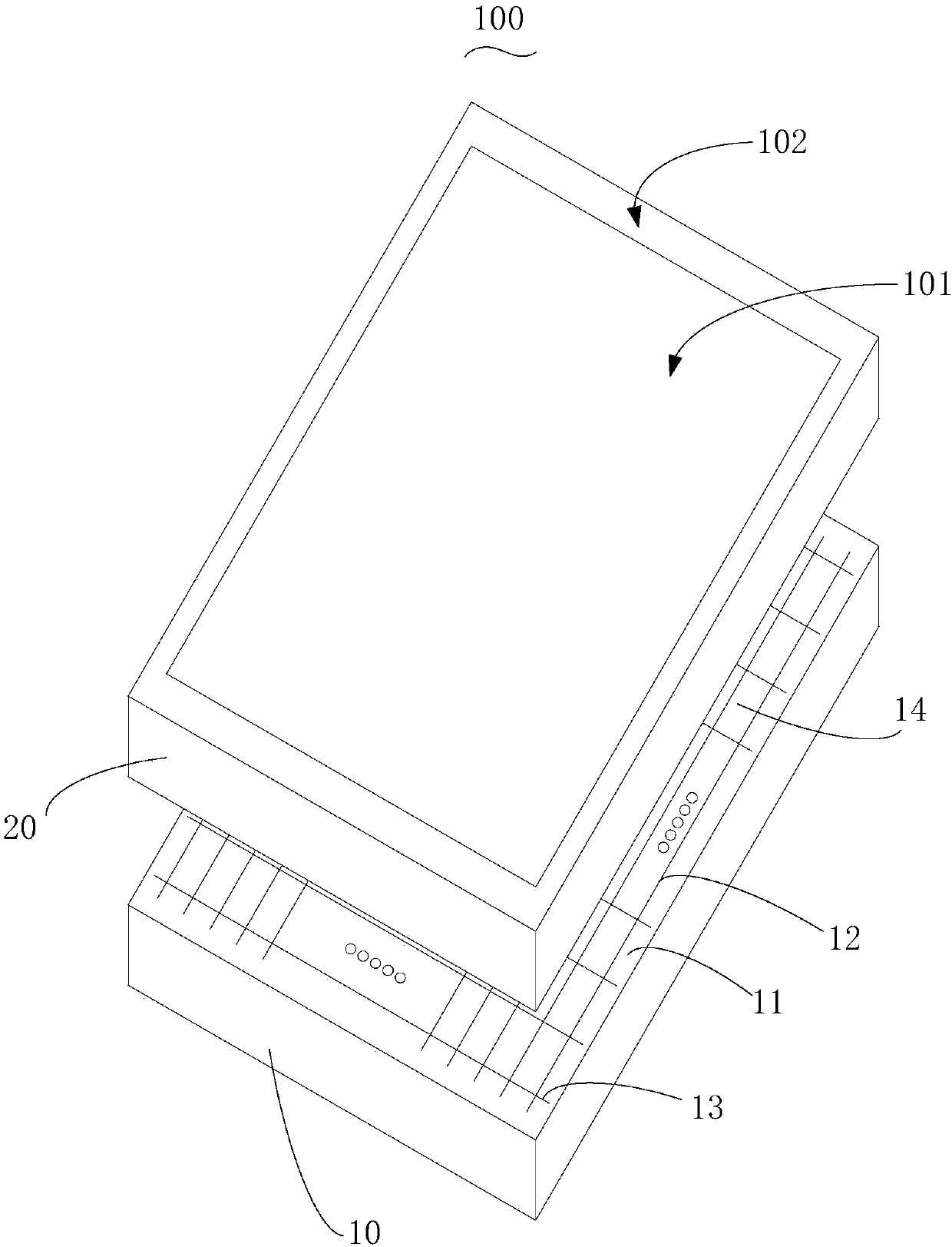
Figure 1 
Figure 2 
Figure 3
Abstract
Description
technical field
[0001] The present invention relates to the field of display technology, in particular to a method for manufacturing an array substrate, the array substrate and a display device. Background technique
[0002] Due to the rise of the global information society and the development of science and technology, the field of display technology is changing with each passing day, and there are more and more types of display technologies, such as traditional liquid crystal display technology, organic light-emitting diode (Organic Light-Emitting Diode, OLED) display technology , electrophoretic display technology, etc. Compared with other displays, the organic electroluminescent diode display has the advantages of self-luminous display, fast response speed, high brightness, wide viewing angle, etc., so that it has a wide application prospect.
[0003] Although the organic electroluminescent diode display technology has the above-mentioned many advantages, in the existin...
Examples
Embodiment Construction
[0019] The following will clearly and completely describe the technical solutions in the embodiments of the present invention with reference to the accompanying drawings in the embodiments of the present invention. Obviously, the described embodiments are some of the embodiments of the present invention, but not all of them. Based on the embodiments of the present invention, all other embodiments obtained by persons of ordinary skill in the art without creative efforts fall within the protection scope of the present invention.
[0020] see figure 1 , figure 1 A perspective view of a display device provided by a preferred embodiment of the present invention. Such as figure 1 As shown, the display device 100 includes an array substrate 10 and an opposite substrate 20, and the array substrate 10 and the opposite substrate 20 are arranged opposite to each other to form a display panel of the display device 100, thereby realizing the display The display function of the device 10...