
low impedance display
A display, low-impedance technology, used in static indicators, instruments, etc., to solve problems such as inability to charge pixels to the expected voltage potential
Patent Information
- Authority / Receiving Office
- CN · China
- Patent Type
- Patents(China)
- Current Assignee / Owner
- Publication Date
- 2022-06-28
Smart Images
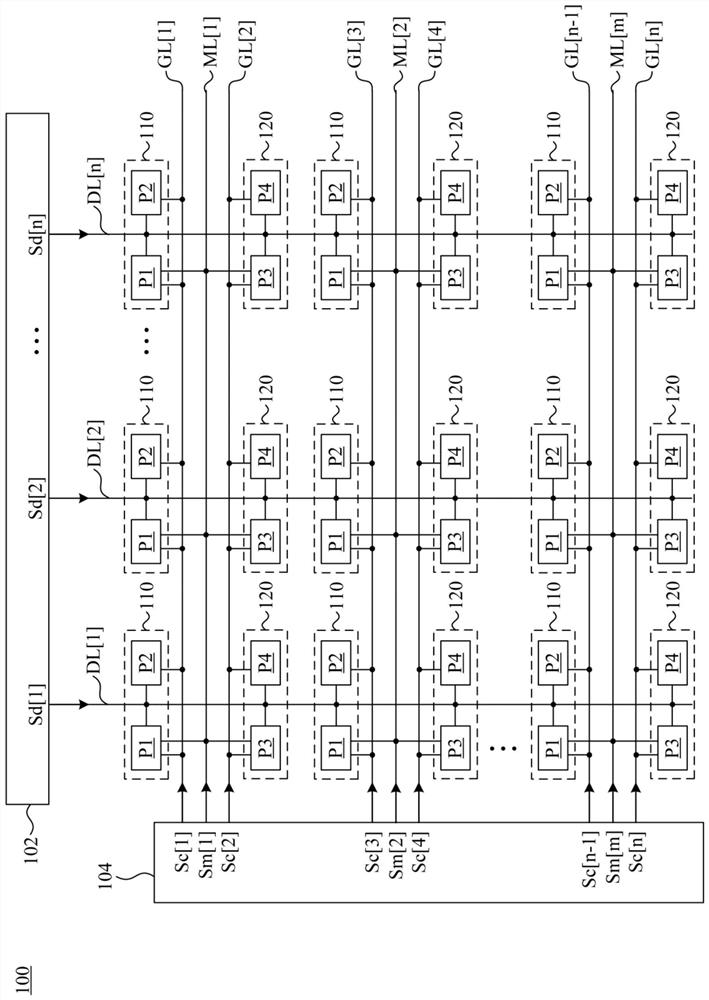
Figure 1 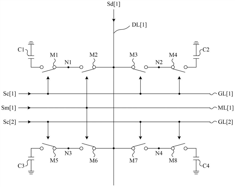
Figure 2 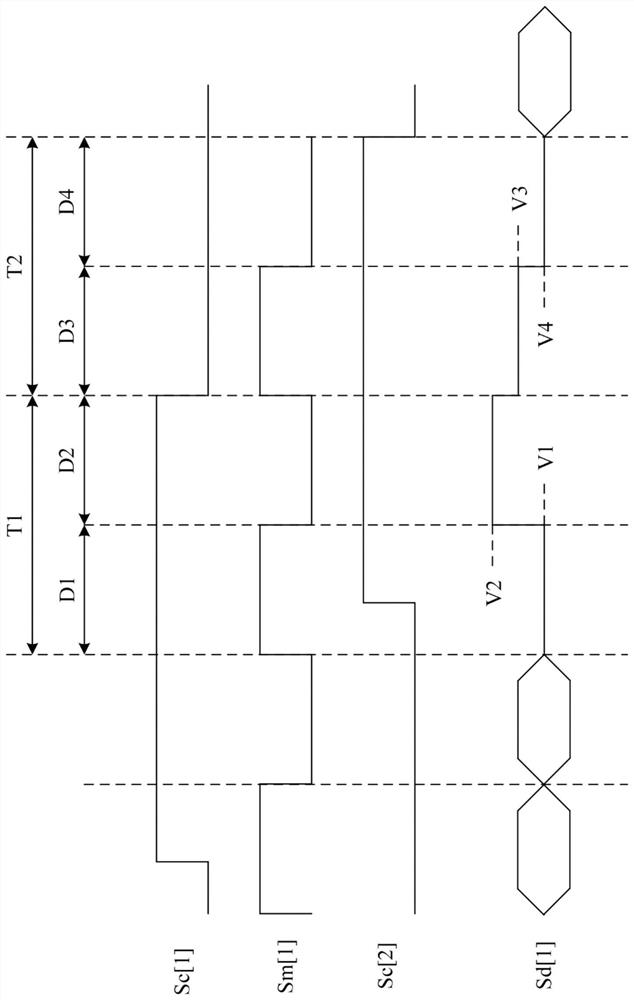
Figure 3
Abstract
Description
technical field
[0001] The present invention relates to a display, in particular to a display that does not need a multiplexer between a source driver and a data line. Background technique
[0002] In order to save cost, a conventional flat panel display will set a multiplexer between the source driver and the data line, so that a larger number of data lines can be driven by the source driver with fewer output pins. However, the multiplexer itself has a high equivalent impedance. Therefore, when a conventional flat panel display has a high resolution or a high frame rate so that each pixel is only allocated a short data writing time, the conventional flat panel display will face the inability to charge the pixel to the desired voltage potential problem.
[0003] In view of this, how to provide a flat panel display that can be applied to high resolution and high frame rate is a problem to be solved in the industry. SUMMARY OF THE INVENTION
[0004] The present invention ...
Examples
Embodiment Construction
[0052] Below in conjunction with accompanying drawing, structure principle and working principle of the present invention are described in detail:
[0053] figure 1 It is a simplified functional block diagram of the low impedance display 100 according to an embodiment of the present invention. The low-impedance display 100 includes a source driver 102, a gate driver 104, a plurality of horizontal driving lines GL[1]-GL[n], a plurality of multiplexing driving lines ML[1]-ML[m], and a plurality of data lines DL[ 1 ]˜DL[n], a plurality of first pixel groups 110 and a plurality of second pixel groups 120 . The first pixel group 110 includes a first pixel P1 and a second pixel P2, and the second pixel group 120 includes a third pixel P3 and a fourth pixel P4. The horizontal driving lines GL[1]-GL[n] are used to receive control signals Sc[1]-Sc[n] from the gate driver 104, respectively. The multiplexing driving lines ML[1]-ML[m] are used for receiving the multiplexing signals Sm[...