
Electronic device
A technology for electronic devices and pixel electrodes, applied in circuits, electrical components, electrical solid devices, etc., can solve problems that affect signal transmission quality and functions that do not meet expectations, so as to reduce signal coupling, improve quality, and reduce the possibility of disconnection Effect
Patent Information
- Authority / Receiving Office
- CN · China
- Patent Type
- Applications(China)
- Current Assignee / Owner
- Publication Date
- 2021-06-25
Smart Images
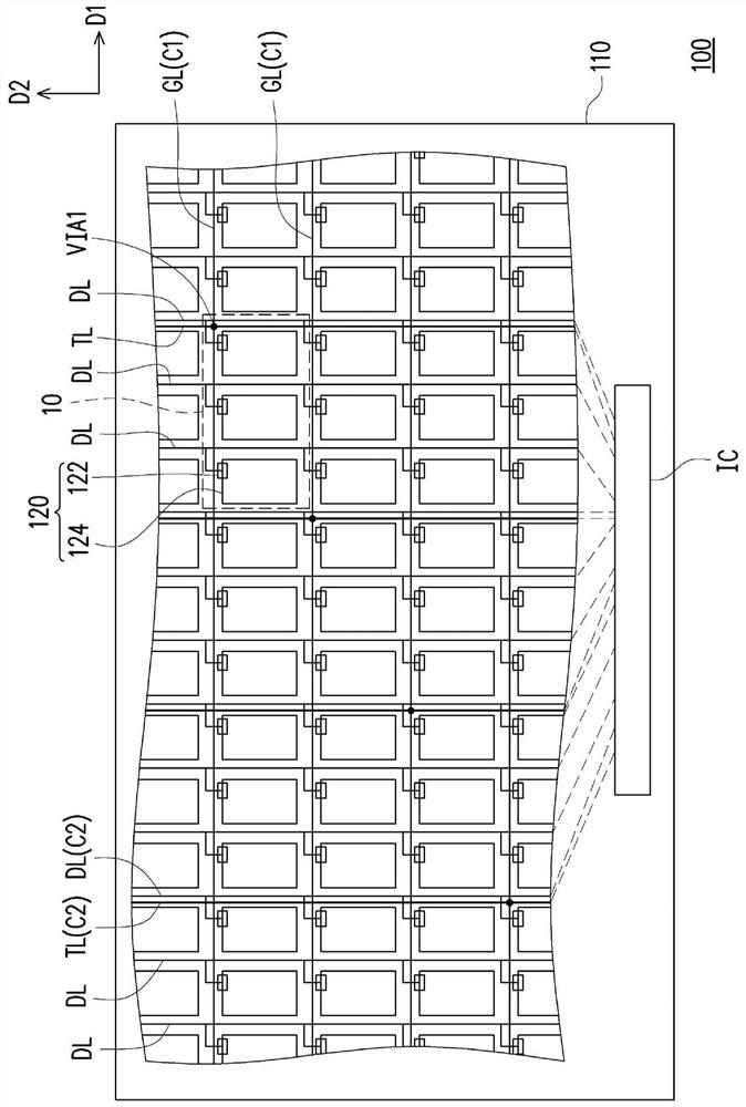
Figure 1 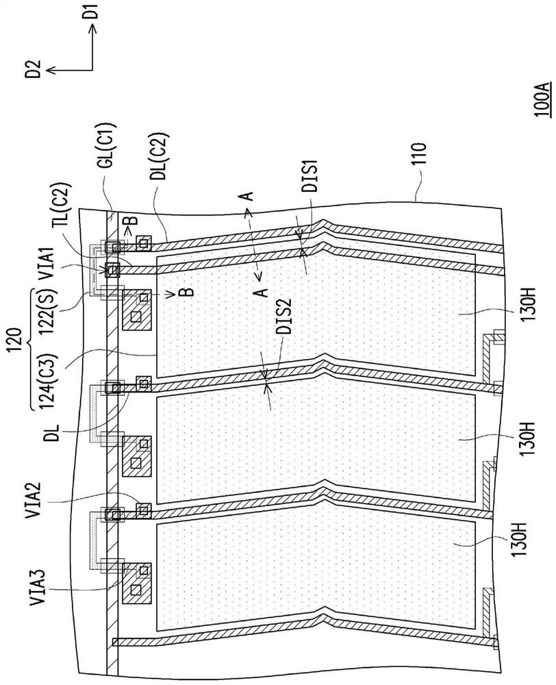
Figure 2 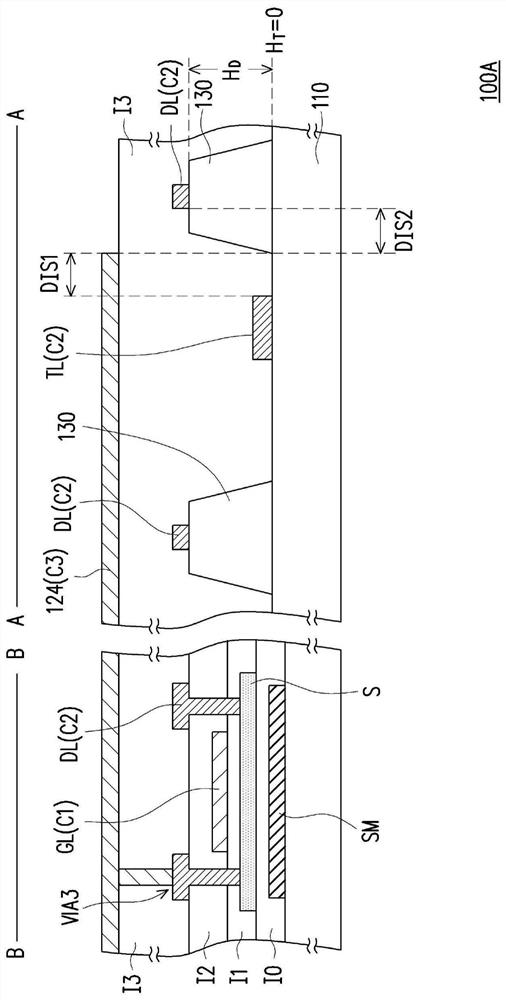
Figure 3
Abstract
Description
technical field
[0001] The invention relates to an electronic device. Background technique
[0002] With the popularization of electronic products, the layout of circuits in various electronic devices is becoming more and more complicated. Therefore, many adjacent lines may be used to carry different types of signals. However, the coupling between adjacent lines often affects the quality of signal transmission, resulting in unexpected functions. Therefore, the planning of circuit layout is often one of the key points in the design of electronic products. Contents of the invention
[0003] The present invention provides an electronic device whose design can help reduce the coupling between lines and provide improved quality.
[0004] The electronic device of the present invention includes a substrate, multiple gate lines, data lines, transfer lines and multiple pixel structures. A plurality of gate lines, data lines, transfer lines and a plurality of pixel structures ar...
Examples
Embodiment Construction
[0053] Reference will now be made in detail to the exemplary embodiments of the present invention, examples of which are illustrated in the accompanying drawings. Wherever possible, the same reference numbers will be used in the drawings and description to refer to the same or like parts.
[0054] It will be understood that when an element such as a layer, film, region, or substrate is referred to as being "on" or "connected to" another element, it can be directly on or connected to the other element, or There may also be intermediate elements between two elements. In contrast, when an element is referred to as being "directly on" or "directly connected to" another element, there are no intervening elements present. As used herein, "connected" may refer to physical and / or electrical connection. Furthermore, "electrically connected" or "coupled" may mean that other elements exist between two elements.
[0055] As used herein, "about," "approximately," or "substantially" incl...