
Display panel, display device and preparation method of display panel
A display panel and substrate technology, applied in semiconductor devices, electrical components, circuits, etc., can solve problems affecting the yield rate of MicroLED displays
Patent Information
- Authority / Receiving Office
- CN · China
- Patent Type
- Applications(China)
- Current Assignee / Owner
- Publication Date
- 2021-10-29
Smart Images
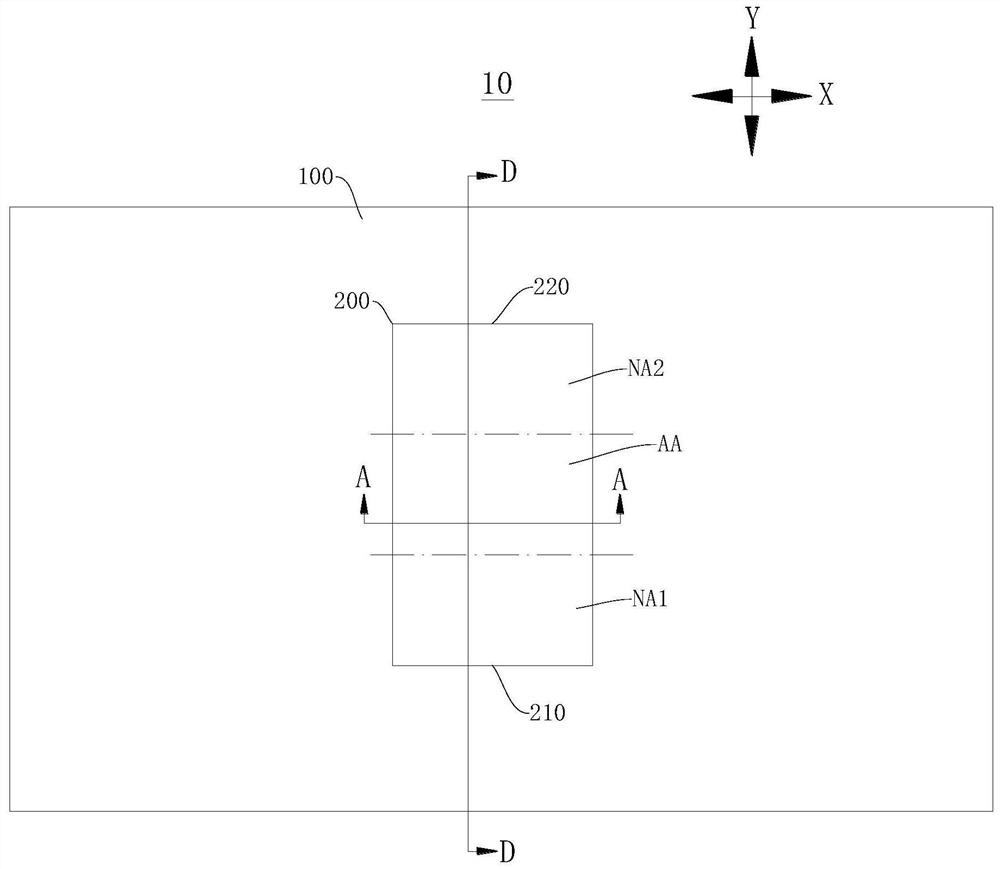
Figure 1 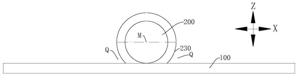
Figure 2 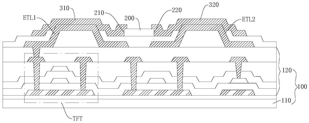
Figure 3
Abstract
Description
technical field
[0001] The present invention relates to the field of display technology, in particular to a display panel, a display device and a method for preparing the display panel. Background technique
[0002] With the continuous development of display technology, people have higher and higher requirements on the service life and display effect of display devices. The light-emitting device of the Micro Light Emitting Diode Display (Micro LED) display is composed of inorganic materials. Compared with the Organic Light Emitting Diode (OLED) display, it has the advantages of high brightness and long life. Therefore, Micro LED displays are gradually becoming the mainstream displays of current display devices.
[0003] The Micro LED display is to form the Micro LED device on the sapphire or silicon substrate or other substrates, and then transfer the Micro LED device to the thin film transistor (Thin Film Transistor, TFT) array substrate through the transfer method, so tha...
Examples
Embodiment Construction
[0034] Features and exemplary embodiments of various aspects of the invention will be described in detail below. In the following detailed description, numerous specific details are set forth in order to provide a thorough understanding of the present invention. It will be apparent, however, to one skilled in the art that the present invention may be practiced without some of these specific details. The following description of the embodiments is only to provide a better understanding of the present invention by showing examples of the present invention. In the drawings and the following description, at least some well-known structures and techniques have not been shown in order to avoid unnecessarily obscuring the present invention; and, for clarity, the dimensions of some structures may have been exaggerated. Furthermore, the features, structures, or characteristics described hereinafter may be combined in any suitable manner in one or more embodiments.
[0035] In the des...