
Package structure and manufacturing method thereof
A packaging structure and manufacturing method technology, applied in the direction of microstructure technology, microstructure devices, manufacturing microstructure devices, etc., can solve the problems of unfavorable packaging structure miniaturization, large area, etc., to achieve miniaturization, increase area, improve Yield and Reliability Effects
Patent Information
- Authority / Receiving Office
- CN · China
- Current Assignee / Owner
- Publication Date
- 2022-07-08
Smart Images
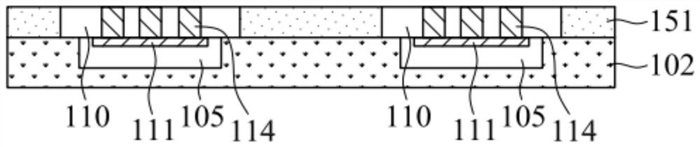
Figure 1 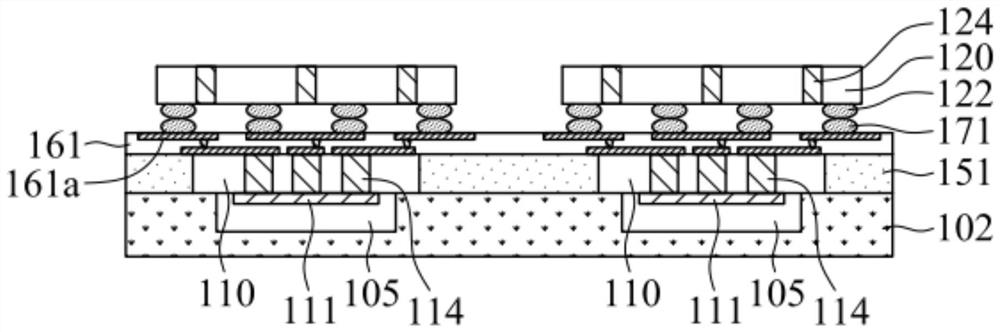
Figure 2 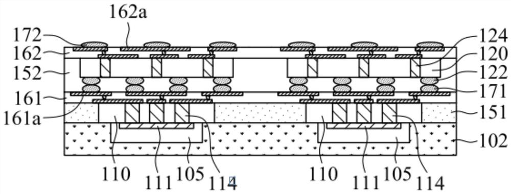
Figure 3
Abstract
Description
technical field
[0001] The present invention relates to a package structure, and more particularly, to a package structure with a three-dimensional MEMS chip stack and a method for manufacturing the same. Background technique
[0002] Microelectromechanical system (microelectromechanical system, MEMS) is a technology that combines microelectronics technology and mechanical engineering. MEMS technology enables the miniaturization of many industrial devices. The MEMS device usually includes a microprocessor and at least one miniature sensor for obtaining external information.
[0003] For current MEMS devices, it is usually necessary to assemble multiple MEMS elements in the same package structure, and to integrate the operations of these MEMS elements. However, if the two MEMS elements are too close, their signals may interfere with each other. As a result, the yield and reliability of the MEMS device will be reduced.
[0004] On the other hand, in the packaging structure...
Examples
Embodiment Construction
[0019] In order to make the above-mentioned and other objects, features and advantages of the present invention more clearly understood, preferred embodiments are given below and described in detail in conjunction with the accompanying drawings. Furthermore, repeated reference symbols and / or wording may be used in different examples of the present invention. These repeated symbols or words are used for the purpose of simplicity and clarity, and are not used to limit the relationship between the various embodiments and / or the described appearance structures.
[0020] The present invention provides a package structure and a manufacturing method thereof, Figures 1A to 1F It is a schematic cross-sectional view of the package structure 100 in various stages of the process according to some embodiments of the present invention.
[0021] Please refer to Figure 1A , a substrate 102 having a plurality of notches 105 is provided. Next, corresponding to the positions of these notches...