
Test circuitry wafer
a test circuit and wafer technology, applied in the field of test circuitry wafers, can solve the problems of increasing the direct cost of manufacturing the probe card/needle, the long lead time needed to manufacture the probe needle, and the high cost of precision probe needle manufacturing, so as to reduce the precision requirement of the probe card, reduce or minimize the number of touchdowns on the device pad, and improve the efficiencies of both testing time and the manufacturing cost of the probe card
Patent Information
- Authority / Receiving Office
- US · United States
- Patent Type
- Applications(United States)
- Current Assignee / Owner
- Publication Date
- 2005-12-29
- Estimated Expiration
- Not applicable · inactive patent
Smart Images
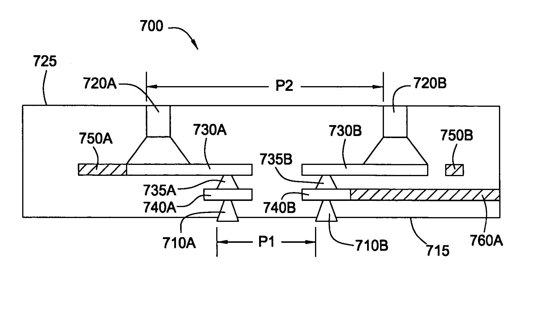
Figure 1 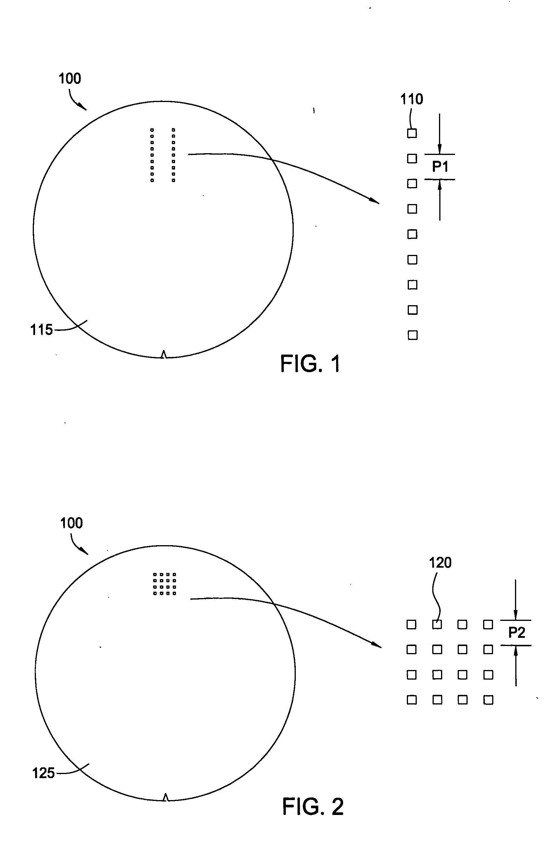
Figure 2 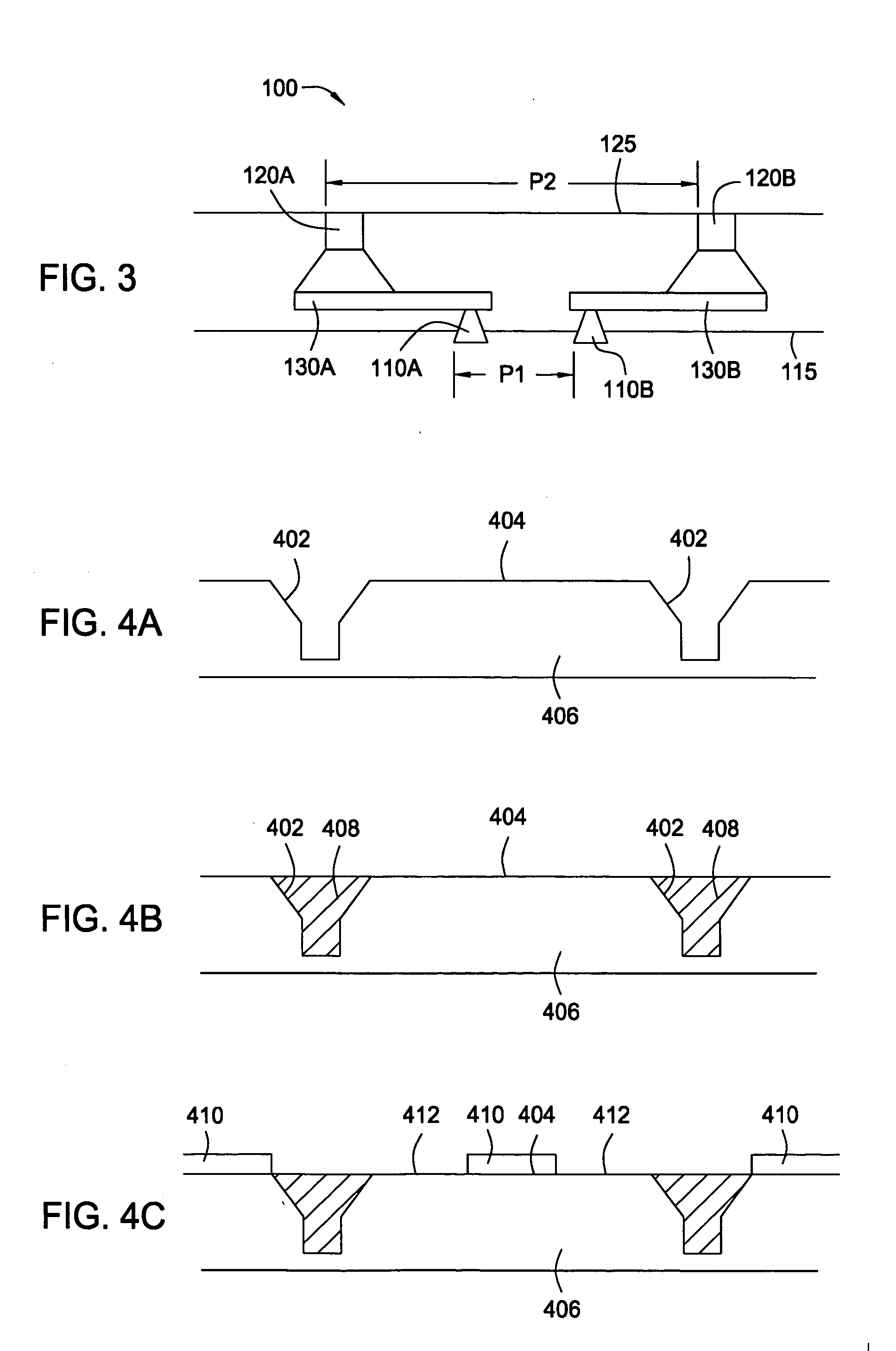
Figure 3
Abstract
Description
BACKGROUND OF THE INVENTION
[0001] 1. Field of the Invention
[0002] The present invention generally relates to an apparatus and method for testing a device wafer having a plurality of devices formed thereon, and more particularly, to an interface for connecting a probe card of a testing system to device pads on a device wafer.
[0003] 2. Description of the Related Art
[0004] In conventional semiconductor manufacturing, a plurality of integrated circuits or devices are formed on a semiconductor substrate or wafer, and after completing the fabrication processes, the devices formed on the wafer may be cut from the wafer and packaged into individual chips, which are then tested individually to ensure that each chip performs according to certain specification. To reduce costs associated with testing chips individually, the devices formed on the wafer may be tested prior to being separated into individual chips. Conducting tests on devices formed on a wafer improves cost efficiencies gener...
Examples
Embodiment Construction
[0030] Embodiments of the present invention generally provide apparatuses and methods for testing a device wafer having a plurality of devices formed thereon. One embodiment provides an interface wafer which serves as an interface between a device wafer having a plurality of devices formed thereon to be tested and a probe card of a testing system. Another embodiment provides a parallel test interface wafer which facilitates parallel testing of devices formed on a device wafer. Yet another embodiment provides a test circuitry wafer which incorporates design-for-test features that are typically implemented on-chip and simplifies device designs by removing the design-for-test features from the device / chip.
[0031] In the following, reference is made to embodiments of the invention. However, it should be understood that the invention is not limited to specific described embodiments. Instead, any combination of the following features and elements, whether related to different embodiments ...