
Cache memory and method for handling effects of external snoops colliding with in-flight operations internally to the cache
a cache memory and internal snoop technology, applied in the field of cache memories in microprocessors, can solve the problems of cache coherence, increase the timing and complexity of the cache control logic to handle the cancelled in-flight operation, and achieve the effect of improving the processing cycle timing and reducing the complexity of other caches
Patent Information
- Authority / Receiving Office
- US · United States
- Patent Type
- Applications(United States)
- Current Assignee / Owner
- Publication Date
- 2006-03-23
Smart Images
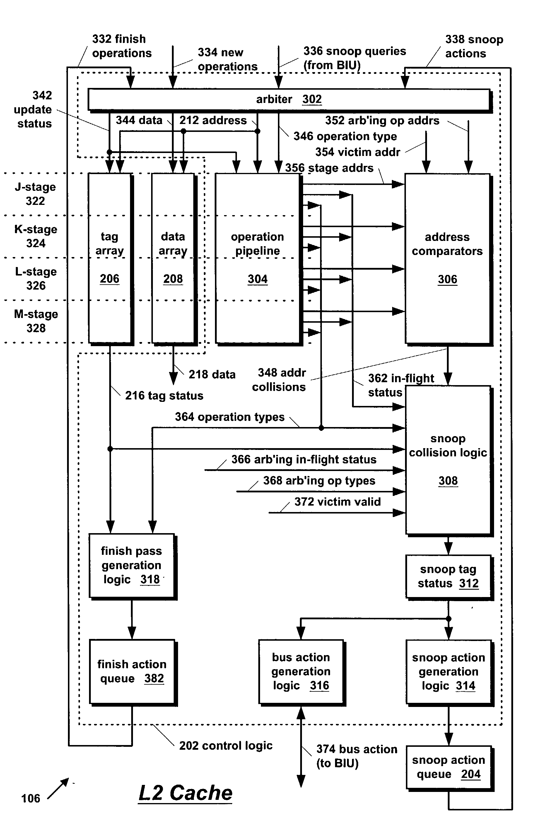
Figure 1 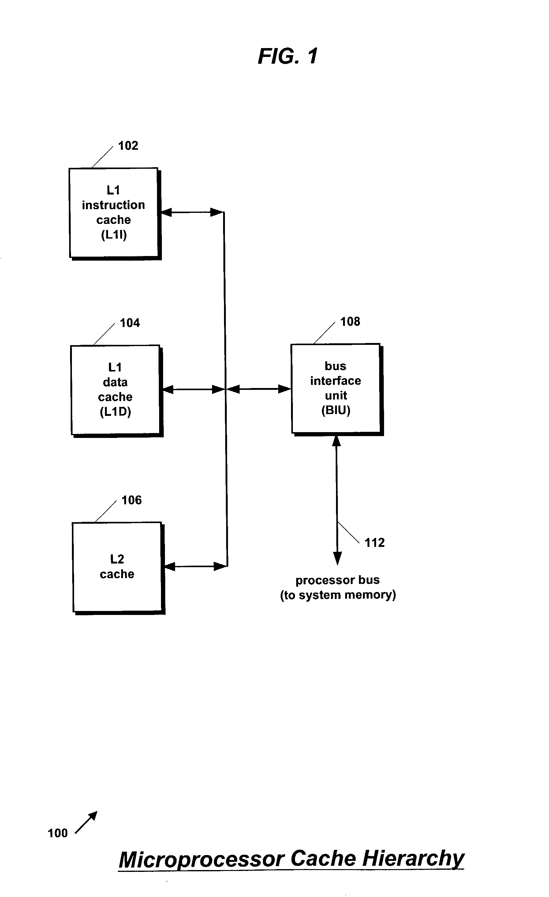
Figure 2 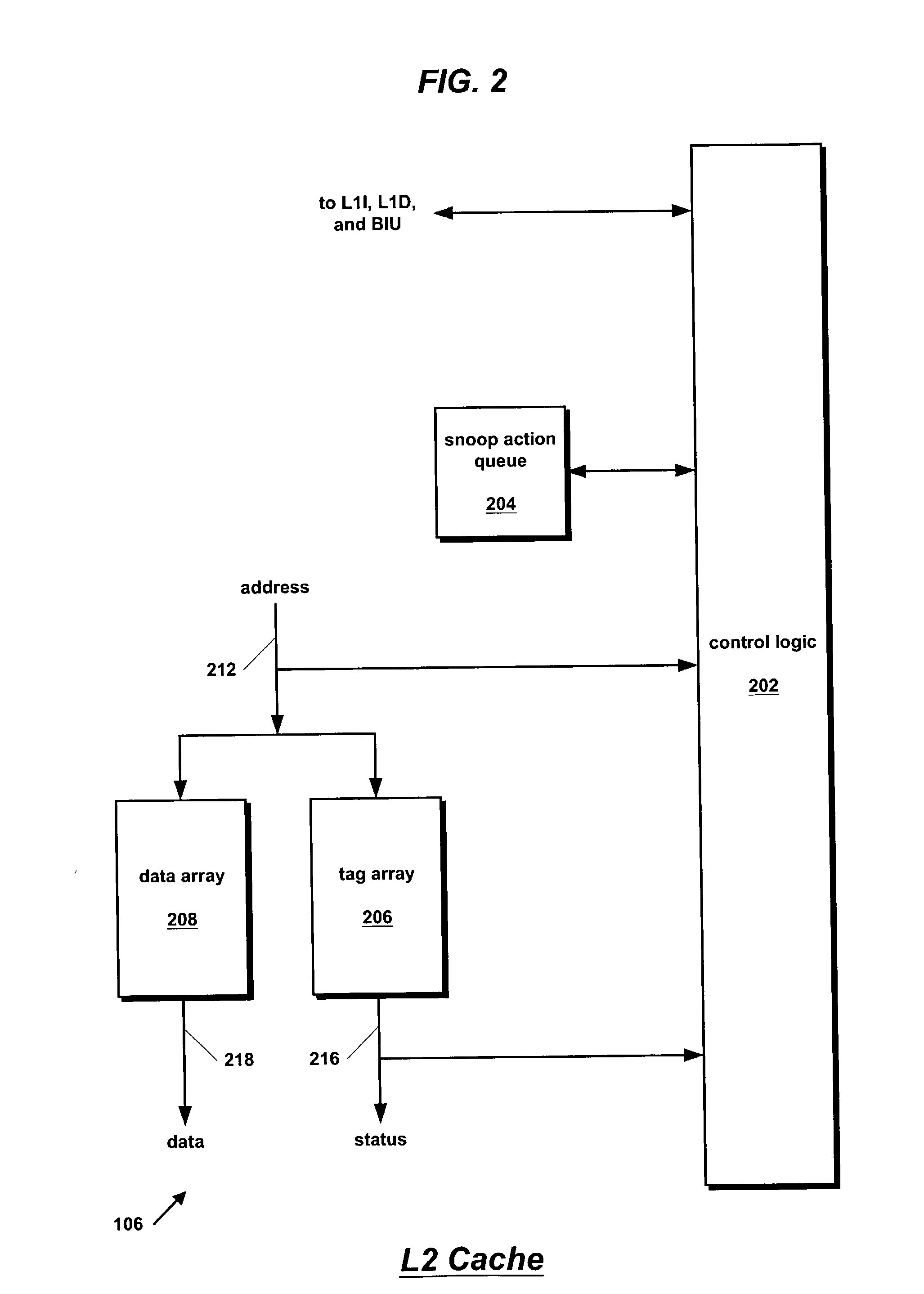
Figure 3
Abstract
Description
[0001] This application claims priority based on U.S. Provisional Application, Serial No. 60 / 375469, filed Apr. 24, 2002, entitled METHOD FOR HANDLING AFFECTS OF EXTERNAL SNOOPS INTERNALLY TO L2 CACHE.FIELD OF THE INVENTION
[0002] This invention relates in general to the field of cache memories in microprocessors, and particularly to multi-pass pipelined caches and the effects of external snoop operations thereon. BACKGROUND OF THE INVENTION
[0003] Many modern computer systems are multi-processor systems. That is, they include multiple processors coupled together on a common bus that share the computing load of the system. In addition, the multiple processors typically share a common system memory. Still further, each of the processors includes a cache memory, or typically a hierarchy of cache memories.
[0004] A cache memory, or cache, is a memory internal to the processor that stores a subset of the data in the system memory and is typically much smaller than the system memory. Tra...
Examples
Embodiment Construction
[0030] Referring now to FIG. 1, a block diagram illustrating a cache hierarchy in a microprocessor 100 according to the present invention is shown.
[0031] Microprocessor 100 comprises a cache hierarchy that includes a level-one instruction (L1I) cache 102, a level-one data (L1D) cache 104, and a level-two (L2) cache 106. The L1I 102 and L1D 104 cache instructions and data, respectively, and L2 cache 106 caches both instructions and data, in order to reduce the time required for microprocessor 100 to fetch instructions and data. L2 cache 106 is between the system memory and the L1I 102 and L1D 104 in the memory hierarchy of the system. The L1I 102, L1D 104, and L2 cache 106 are coupled together. The L1I 102 and L2 cache 106 transfer cache lines between one another, and the L1D 104 and L2 cache 106 transfer cache lines between one another. For example, the L1I 102 and L1D 104 may castout cache lines to or load cache lines from L2 cache 106.
[0032] Microprocessor 100 also includes a bu...