
Method and apparatus for layout independent test point placement on a printed circuit board
Patent Information
- Authority / Receiving Office
- US · United States
- Current Assignee / Owner
- Publication Date
- 2006-04-27
Smart Images
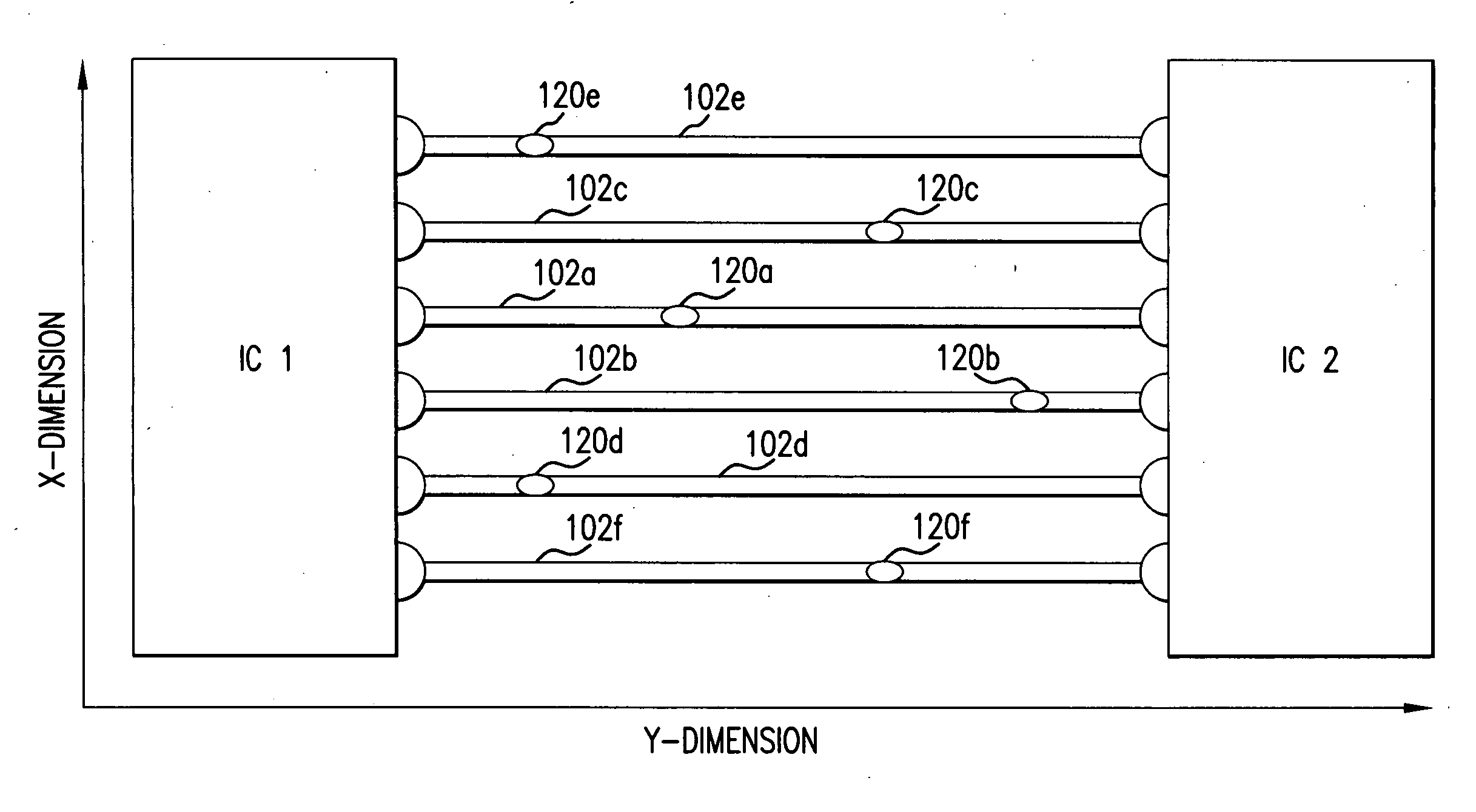
Figure 1 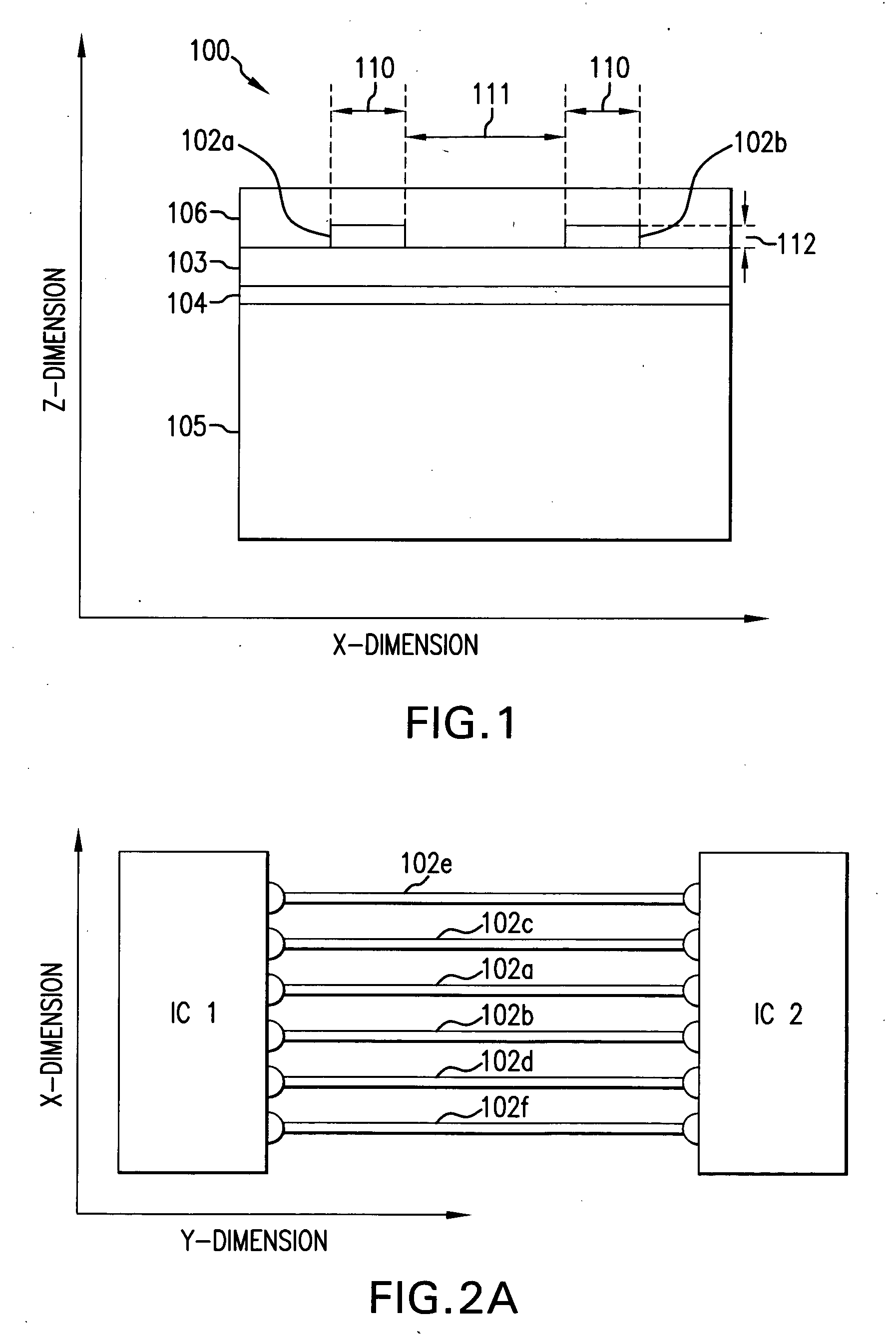
Figure 2 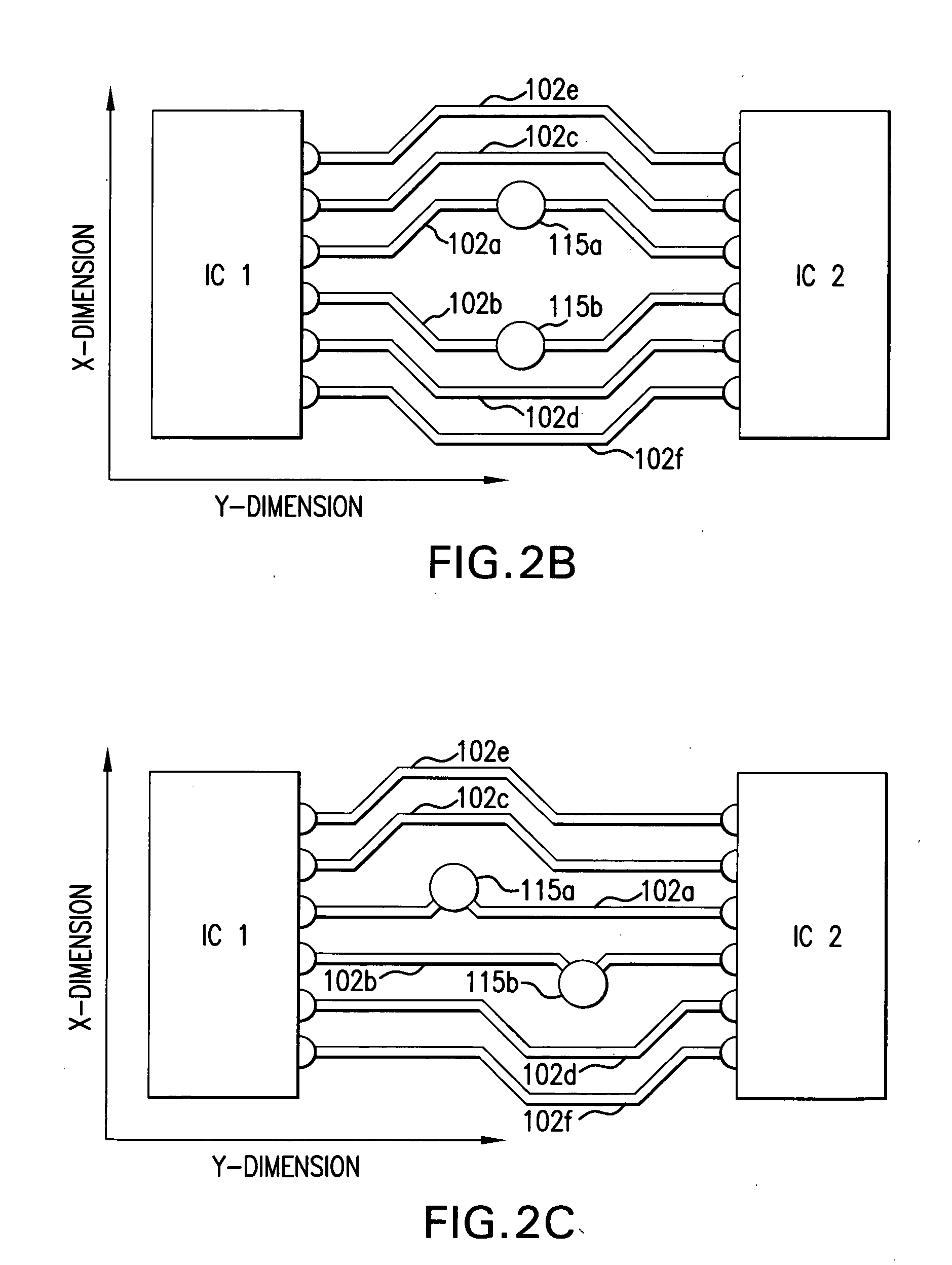
Figure 3
Abstract
Description
REFERENCE TO RELATED PATENT DOCUMENTS
[0001] The subject matter of this patent application is related to that of U.S. patent application Ser. No. 10 / 670,649 entitled Printed Circuit Board Test Access Point Structures And Methods For Making The Same filed Sep. 24, 2003 by Kenneth P. Parker, Ronald J. Peiffer and Glen E. Leinbach and assigned to Agilent Technologies, Inc., which teaches the basic concepts of bead probes or test access point structures on a printed circuit board and is hereby incorporated herein by reference.BACKGROUND OF THE INVENTION
[0002] Printed circuit assemblies (PCA's) are typically tested after manufacture to verify the continuity of traces between pads and vias on the board and to verify that components loaded on the PCA perform within specifications. Such printed circuit assembly testing is generally performed with automated in-circuit testers or ICT's and requires complex tester resources. The tester hardware must generally be capable of probing conductive ...
Examples
Embodiment Construction
[0036] Turning now in detail to the invention, on a trace defined in an x-, y-, z-coordinate system where the x-dimension represents the trace width, the y-dimension represents the trace length, and the z-dimension represents the trace thickness, it will be recognized by those skilled in the art that present techniques for test access point placement on a printed circuit board utilize only the x- and y-dimensions. The present invention takes a different approach by taking advantage of the z-dimension, that is, the trace thickness. In this regard, the test access point structure of the invention is a localized “high point” on a printed circuit board trace that does not significantly perturb the impedance of the trace and that can be targeted with a probe. Throughout this specification, test access point structure and bead probe structure are used interchangeably.
[0037]FIG. 3 illustrates an exemplary embodiment of a test access point structure implemented in accordance with the inven...