
Method and apparatus for updating wide storage array over a narrow bus
a technology of a wide storage array and a bus, applied in the field of computer systems, can solve the problems of inability to count more than n events at the same time, inability to update the data storage array, and inability to meet the needs of large-scale data storage, so as to reduce the area required, and reduce the size of the area.
Patent Information
- Authority / Receiving Office
- US · United States
- Patent Type
- Applications(United States)
- Current Assignee / Owner
- Publication Date
- 2008-05-29
- Estimated Expiration
- Not applicable · inactive patent
Smart Images
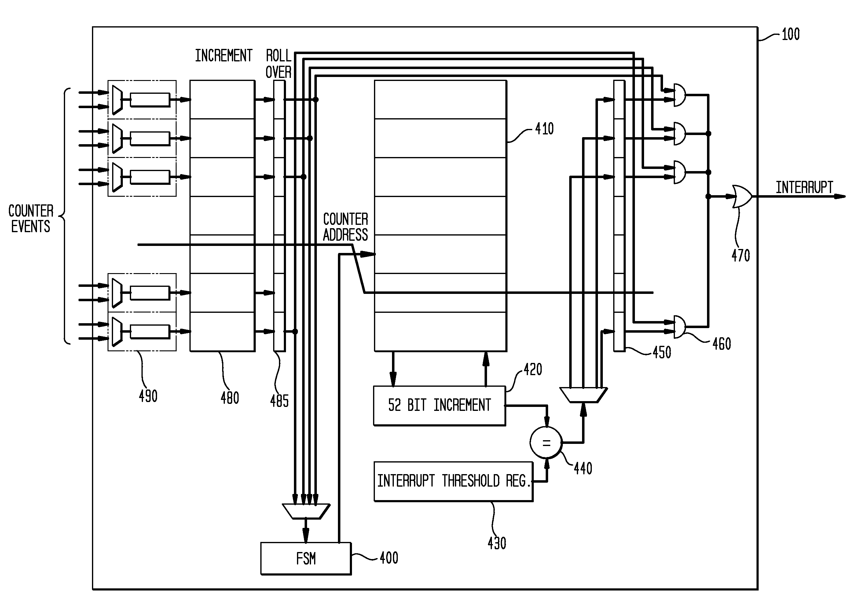
Figure 1 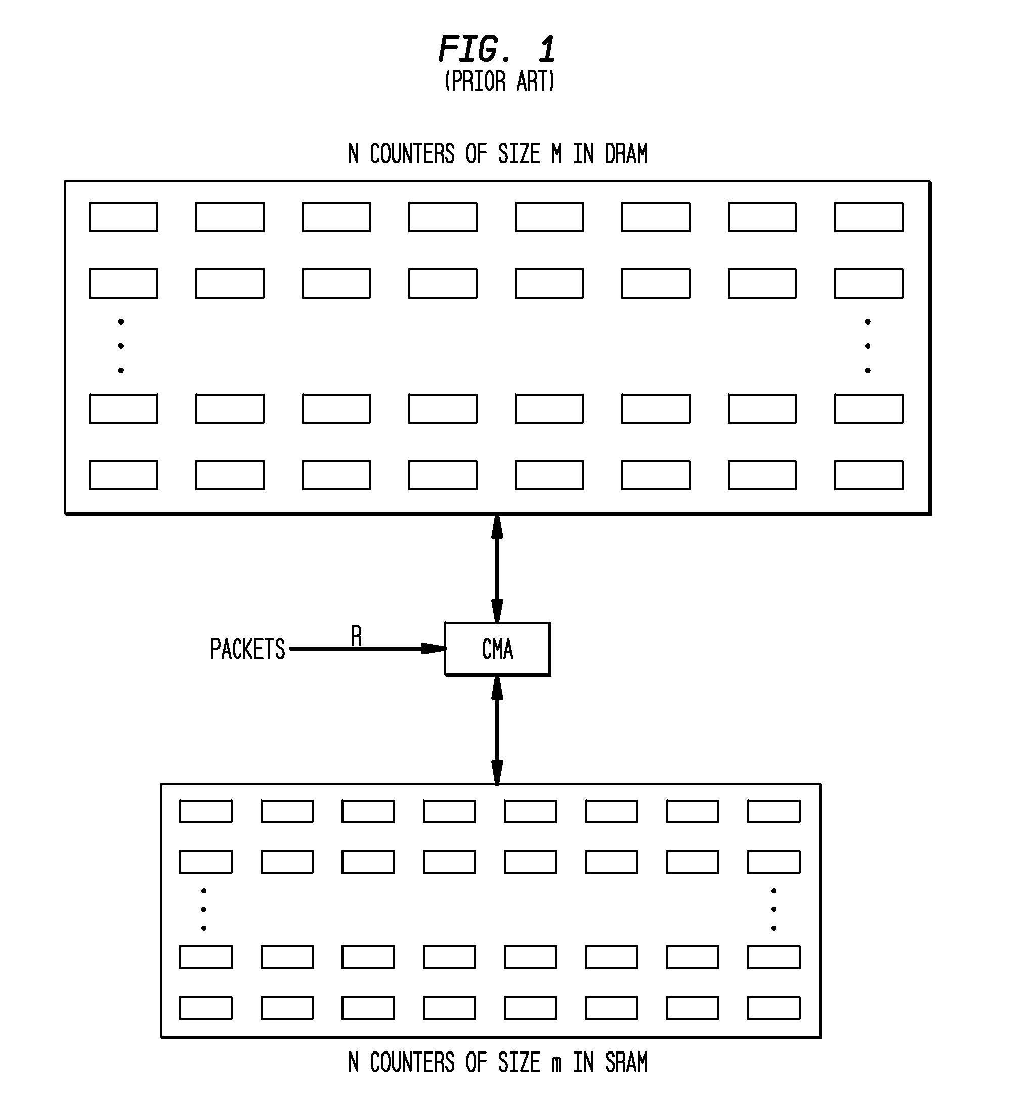
Figure 2 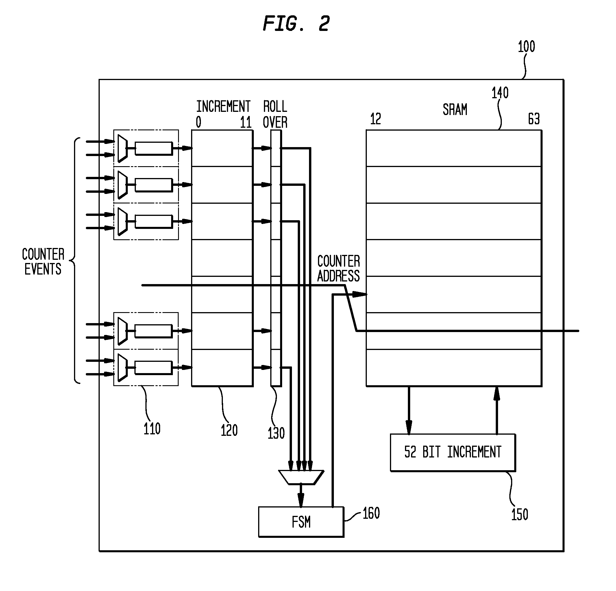
Figure 3
Abstract
Description
CROSS-REFERENCE TO RELATED APPLICATIONS
[0001] The present application relates to commonly-owned, co-pending U.S. patent applications Ser. No. ______ [Docket No. 19829; YOR920060335US1]; Ser. No. ______ [Docket No. 19830; YOR9200600336US1] and, Ser. No. ______ [Docket No. 19832; YOR920060338US1], each of which was filed on even date herewith.BACKGROUND OF THE INVENTION
[0002] 1. Field of the Invention
[0003] The present invention generally relates to computer systems using single or multiprocessor architectures and, more particularly, to a novel implementation for communicating data from a bus to a wide data storage array, wherein the bus is of a narrow data width as compared to the data width of the array to which data is to be transferred.
[0004] 2. Description of the Prior Art
[0005] Many processor architectures include on a chip a set of counters that allow counting a series of processor events and system events on the chip, such as cache misses, pipeline stalls and floating point operati...
Examples
Embodiment Construction
[0060]Referring now to drawings, and more particularly to FIG. 2, there is depicted a preferred embodiment of the invention. The performance counter unit 100 contains N of counters. The N counter events to monitor are selected from set of M events selected by the set of N multiplexers 110. The selected performance events are counted in the counter block 120, which implements N counters which are n width representing n least significant bits of a counter. The counters in the block 120 are implemented using discrete registers. In the preferred embodiment, the block 120 implements only lowest 12 bits of 64-bit counters, but it would be obvious to skilled artisans that any number of lower bits can be counted in the discrete register logic block.
[0061]When a counter from the counter block 120 reaches its maximum, its value rolls over to zero, and the corresponding bit in the “roll over bit” block 130 is set, and the counter continues to track performance events.
[0062]The K−n most signifi...