
Method for adhering semiconductor devices
a technology of semiconductor devices and semiconductor components, applied in semiconductor devices, semiconductor/solid-state device details, electrical apparatus, etc., can solve the problems of deteriorating electrical and physical properties of semiconductor devices, cracking of deep via conductors, and difficult realization of various devices having different design rules on one chip, so as to prevent cracking of semiconductor devices, wide area, and dissipate thermal energy generated by semiconductor devices
Patent Information
- Authority / Receiving Office
- US · United States
- Patent Type
- Applications(United States)
- Current Assignee / Owner
- Publication Date
- 2008-11-20
- Estimated Expiration
- Not applicable · inactive patent
Smart Images
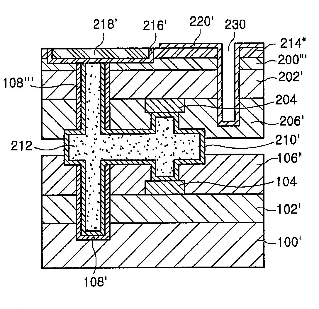
Figure 1 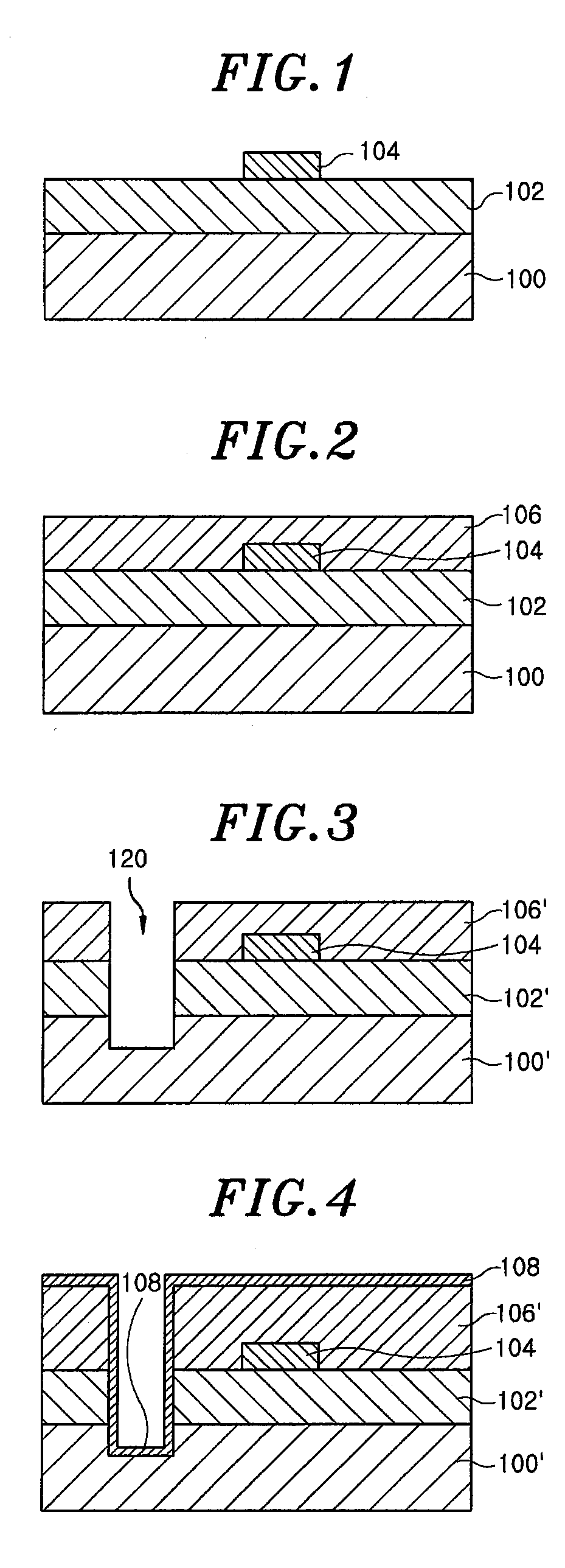
Figure 2 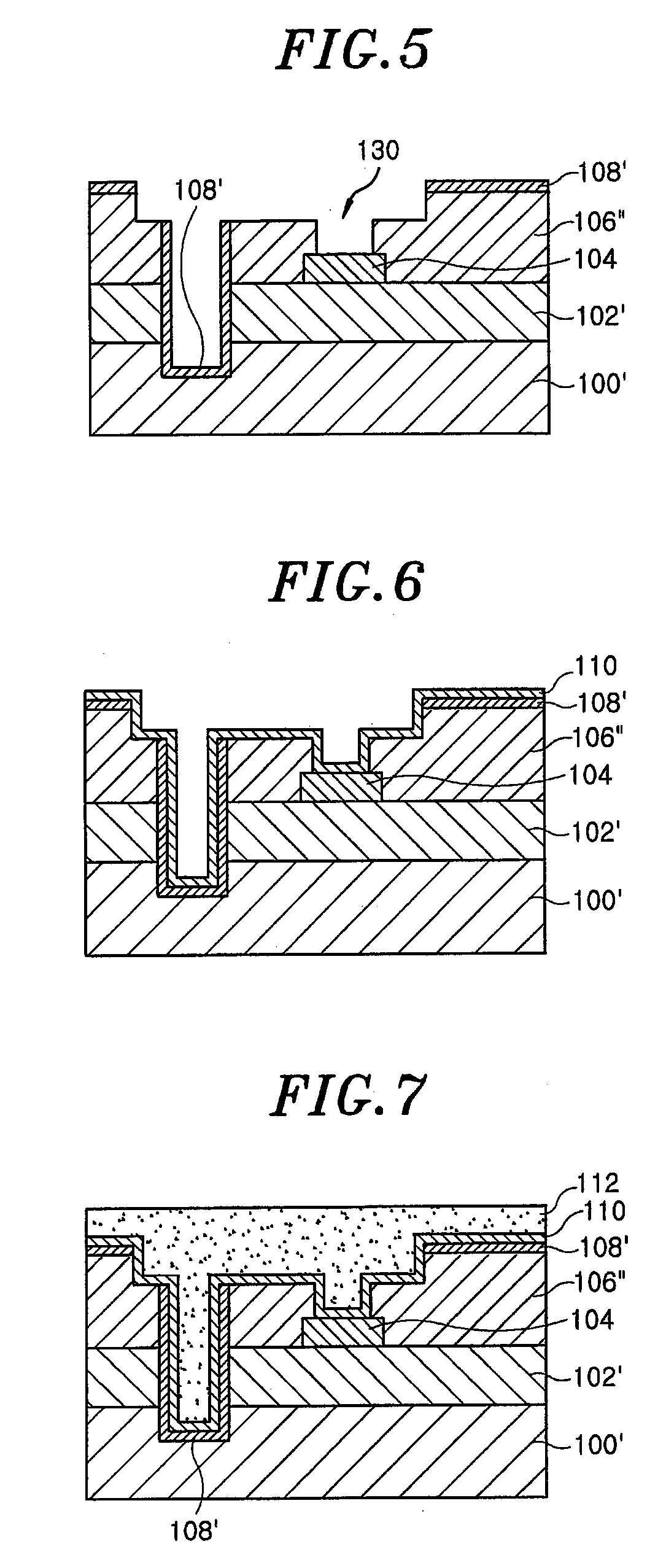
Figure 3
Abstract
Description
TECHNICAL FIELD
[0001] Embodiments consistent with the present invention relate to a method for adhering semiconductor devices, and more particularly, to a method for adhering semiconductor devices capable of preventing a crack phenomenon.RELATED ART
[0002] In the semiconductor industry, for example, in system on chip (SOC) technology, researchers have attempted to integrate analog, RF, CPU, and CMOS sensors on one chip. However, realizing various devices having different design rules on one chip is very difficult and has many limitations.
[0003] In order to solve such a problem, a system in package (SIP) technology has been introduced. In SIP, two different semiconductor devices are connected to each other by a deep via conductor to reduce chip size and to secure enough storage capacity.
[0004] Generally, semiconductor devices are connected through deep via conductors having a high aspect ratio. Heat generated by a multi-level chip accumulates in the semiconductor devices, and can easily d...
Examples
Embodiment Construction
[0010]Hereinafter, embodiments consistent with the present invention will be described in detail with reference to the accompanying drawings so that they can be readily implemented by those skilled in the art.
[0011]FIGS. 1 to 17 are sectional views illustrating a method for adhering semiconductor devices in accordance with one embodiment consistent with the present invention.
[0012]Specifically, FIGS. 1 to 9 illustrate a process for manufacturing a first semiconductor device consistent with the present invention and FIGS. 10 to 17 illustrate a process for forming a heat sink when a second semiconductor device consistent with the present invention is adhered to the first semiconductor device. As illustrated in FIGS. 1 and 2, after depositing an insulating layer 102 on a semiconductor substrate 100, an upper metal layer 104 is formed on insulating layer 102 and a gap fill layer 106 is formed on upper metal layer 104 and insulating layer 102. In one embodiment, insulating layer 102 may ...