
Resin-seal type semiconductor device
a semiconductor device and sealing technology, applied in semiconductor devices, semiconductor/solid-state device details, electrical devices, etc., can solve the problems of increasing power consumption and integration of semiconductor devices, difficult to adequately dissipate heat generated in semiconductor chips, and increasing the heat generation of semiconductor devices in operation, so as to prevent reliability from deteriorating, the heat dissipation characteristic is further improved
Patent Information
- Authority / Receiving Office
- US · United States
- Patent Type
- Applications(United States)
- Current Assignee / Owner
- Publication Date
- 2009-07-23
Smart Images
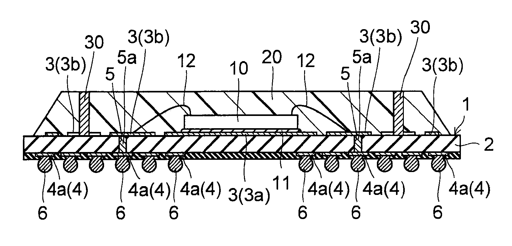
Figure 1 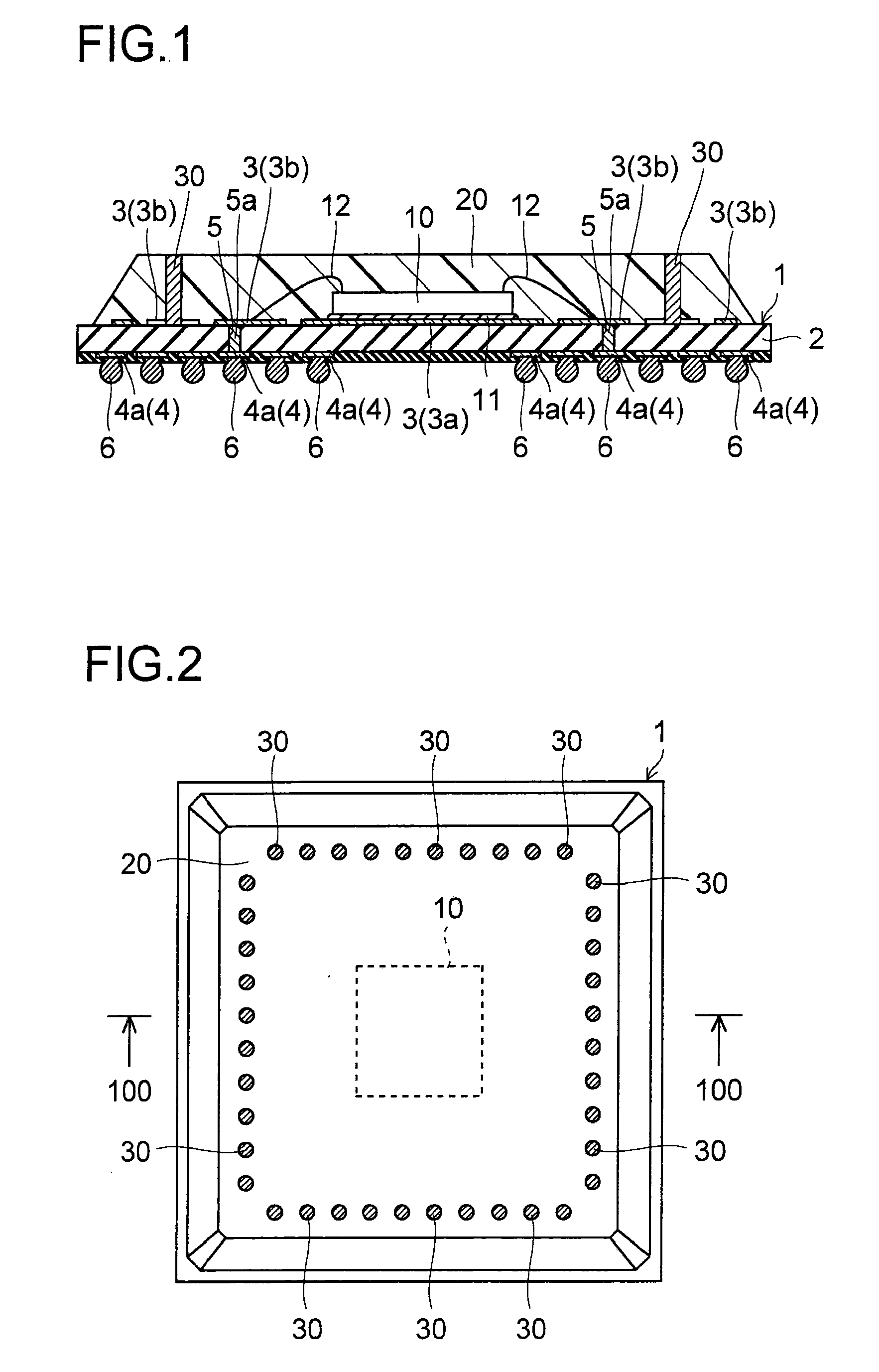
Figure 2 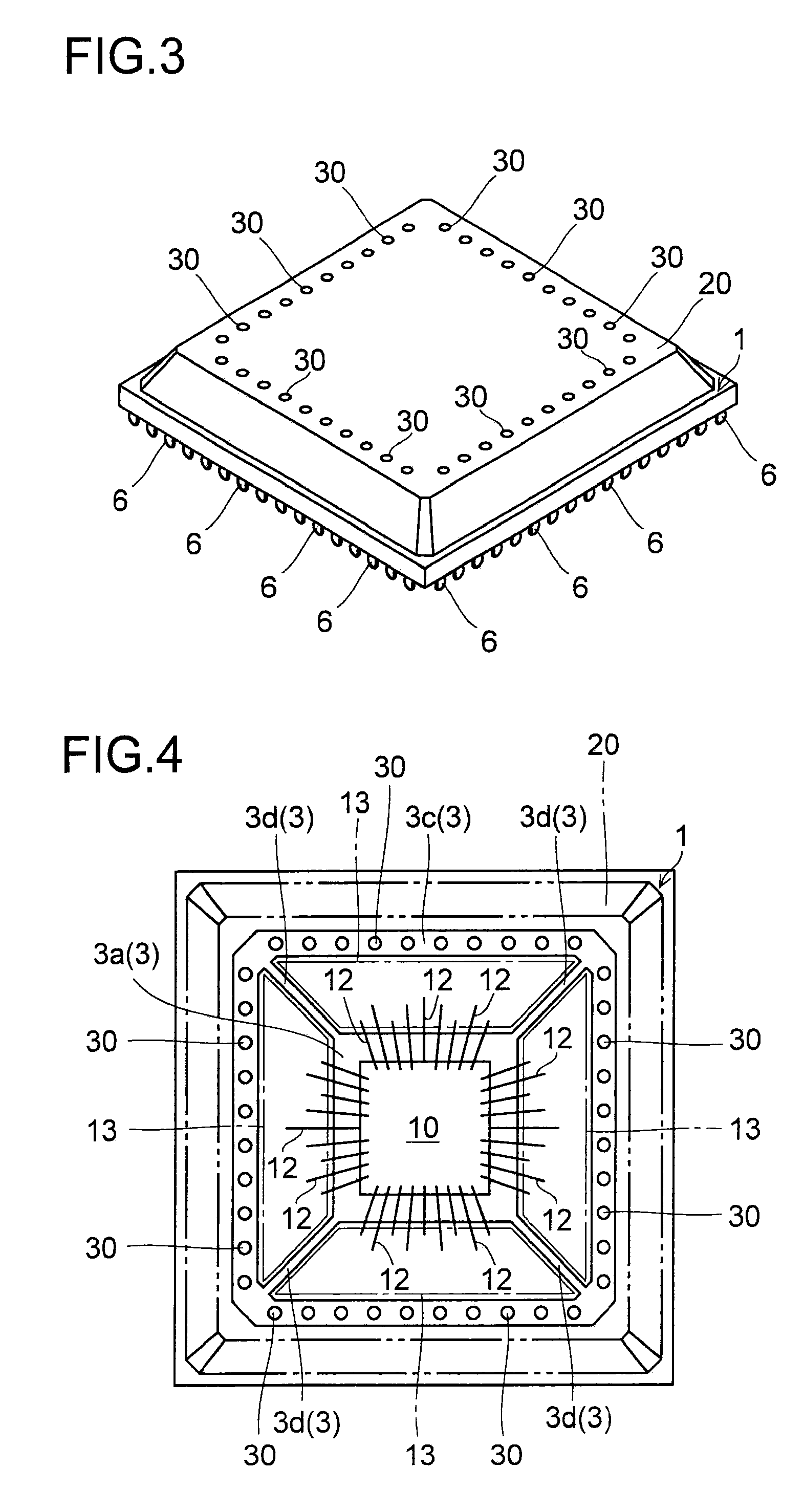
Figure 3
Abstract
Description
[0001] This application is based on Japanese Patent Application No. 2007-277269 filed on Oct. 25, 2007, the contents of which are hereby incorporated by reference.BACKGROUND OF THE INVENTION
[0002] 1. Field of the Invention
[0003] The present invention relates to a resin-seal type semiconductor device, and particularly relates to a resin-seal type semiconductor device having a substrate on which a semiconductor chip is mounted.
[0004] 2. Description of Related Art
[0005] Along with the recent increase in power consumption and integration of semiconductor devices, semiconductor devices have come to generate more heat in operation. Since such increase in heat generated by semiconductor devices in operation causes problems such as a malfunction and a shorter lifetime of a semiconductor element, there has been strong demand for improvement in heat dissipating characteristic of semiconductor devices.
[0006] A conventionally known way of meeting such demand is use of a resin-seal type semiconductor ...
Examples
first embodiment
[0027]FIG. 1 is a sectional view showing a BGA type semiconductor device of a first embodiment of the present invention. FIG. 2 is a plan view showing the BGA type semiconductor device of the first embodiment of the present invention. FIG. 3 is an overall perspective view showing the BGA type semiconductor device of the first embodiment of the present invention. FIG. 1 is a sectional view taken along line 100-100 in FIG. 2. First, a description will be given of a structure of the BGA type semiconductor device of the first embodiment of the present invention, with reference to FIGS. 1 to 3.
[0028]The BGA type semiconductor device according to the first embodiment at least includes, as shown in FIG. 1, a wiring substrate 1, a semiconductor chip 10 that is mounted on the wiring substrate 1, and a sealing resin layer 20 that covers the semiconductor chip 10 at a top face of the wiring substrate 1. The wiring substrate 1 is an example of the “substrate” of the present invention.
[0029]The ...
second embodiment
[0043]FIG. 5 is a sectional view showing a BGA type semiconductor device of a second embodiment of the present invention. As shown in FIG. 5, the BGA type semiconductor device of this second embodiment is the BGA type semiconductor device of the first embodiment described above further including a heat sink 40. This heat sink 40 is formed of a metal material such as aluminum that is highly thermally conductive, and it has a plurality of heat dissipating fins 41. The heat sink 40 is fixed to the top face of the sealing resin layer 20 such that it is thermally connected to each one of the plurality of metal bumps 30.
[0044]Incidentally, the second embodiment is otherwise structured in the same manner as the first embodiment described above.
[0045]In the second embodiment, as a result of the heat sink 40 that is thermally connected to the metal bumps 30 being provided on the top face of the sealing resin layer 20 as described above, heat generated in the semiconductor chip 10 can be effe...
third embodiment
[0047]FIG. 6 is a sectional view showing a BGA type semiconductor device of a third embodiment of the present invention. As shown in FIG. 6, in this BGA type semiconductor device of the third embodiment, at least one of the plurality of metal bumps 30 is formed to be electrically connected to a predetermined one of the connection electrode layers 3b. This enables the at least one of the metal bumps 30 that is electrically connected to the predetermined one of the connection electrode layers 3b to function as an electric conductor.
[0048]With the BGA type semiconductor device of the third embodiment structured as described above, when another semiconductor device 50 is mounted on the BGA type semiconductor device to form a package-on-package (PoP) structure, the upper-side semiconductor device 50 can be electrically connected to the lower-side BGA type semiconductor device easily. And in a case where the semiconductor device 50 that is placed on the upper side is provided with heat di...