
Solid state storage system using global wear leveling and method of controlling the solid state storage system
a solid state storage and wear leveling technology, applied in the direction of memory address/allocation/relocation, instruments, computing, etc., can solve the problems of data not being uniformly programmed, memory cells may become worn out, and the overall performance of the solid state storage system may be restricted
Patent Information
- Authority / Receiving Office
- US · United States
- Current Assignee / Owner
- Publication Date
- 2010-04-08
- Estimated Expiration
- Not applicable · inactive patent
Smart Images
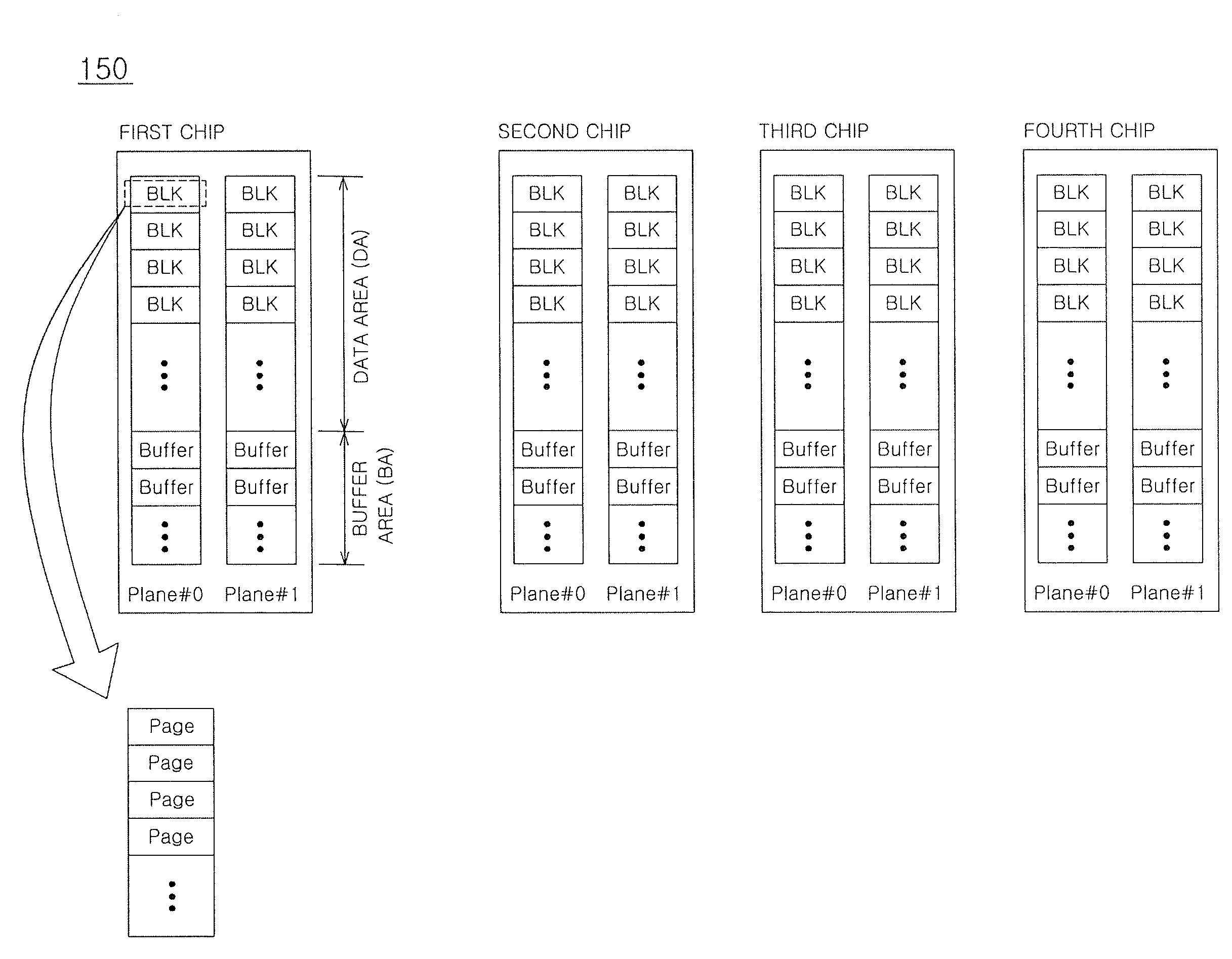
Figure 1 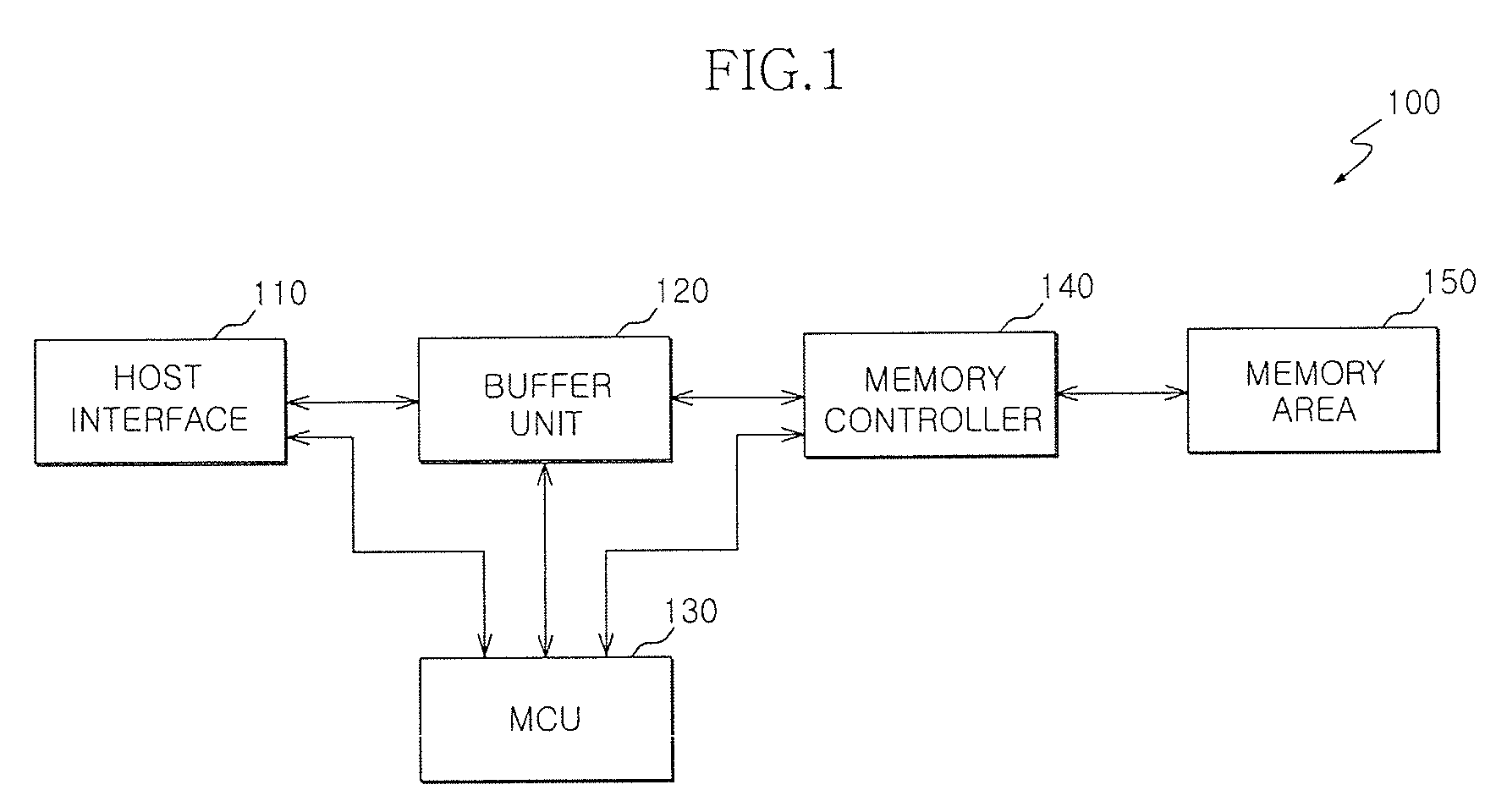
Figure 2 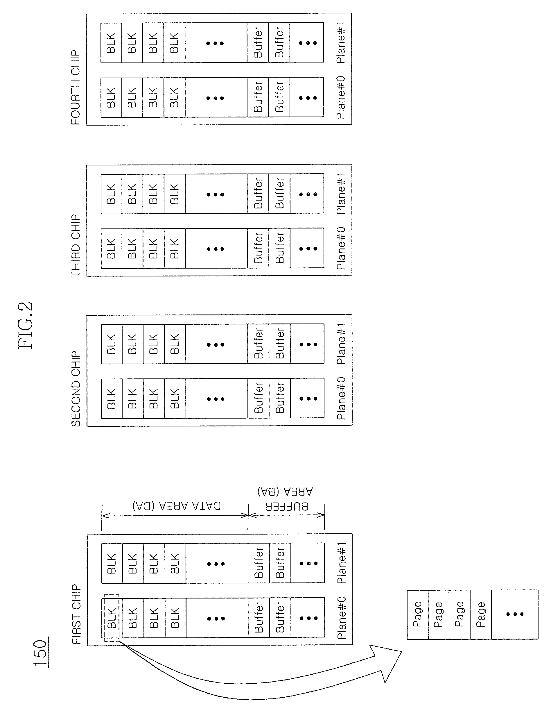
Figure 3
Abstract
Description
CROSS-REFERENCES TO RELATED PATENT APPLICATION
[0001] The present application claims priority under 35 U.S.C 119(a) to Korean Application No. 10-2008-0097184, filed on Oct. 2, 2008, in the Korean Intellectual Property Office, which is incorporated herein by reference in its entirety as set forth in full.BACKGROUND
[0002] 1. Technical Field
[0003] The present invention described herein relates generally to a solid state storage system and a method of controlling the solid state storage system, and more particularly, to a solid state storage system that can control allocation of memory blocks and a method of controlling the solid state storage system.
[0004] 2. Related Art
[0005] In recent years, solid state storage systems, such as solid state drives (SSD) that use NAND flash memories, have introduced various algorithms and control methods to improve system performance.
[0006] In a solid state storage system, data is repeatedly written and updated to NAND flash memory cells.
[0007] In general, whe...
Examples
Embodiment Construction
.”
BRIEF DESCRIPTION OF THE DRAWINGS
[0018]Features, aspects, and embodiments of the present invention are described in conjunction with the attached drawings, in which:
[0019]FIG. 1 is a block diagram showing an exemplary solid state storage system according to one embodiment;
[0020]FIG. 2 is a block diagram showing a hierarchical structure of an exemplary memory area that can be included with the system according to one embodiment of the present invention;
[0021]FIG. 3 is a conceptual block diagram showing a logical block address mapping relationship according to one embodiment of the present invention; and
[0022]FIG. 4 is a conceptual block diagram showing a mapping relationship between logical block addresses and physical block addresses according to one embodiment of the present invention;
[0023]FIG. 5 is a block diagram showing a delete management table of logical blocks and a delete management table of physical blocks according to one embodiment of the present invention:
[0024]FIG. 6...