
Wiring board and method of manufacturing the same
Patent Information
- Authority / Receiving Office
- US · United States
- Current Assignee / Owner
- Publication Date
- 2012-06-21
- Estimated Expiration
- Not applicable · inactive patent
Smart Images
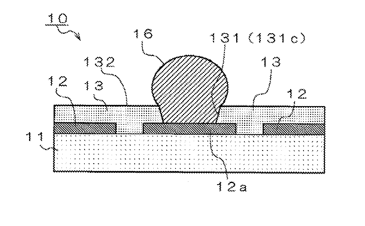
Figure 1 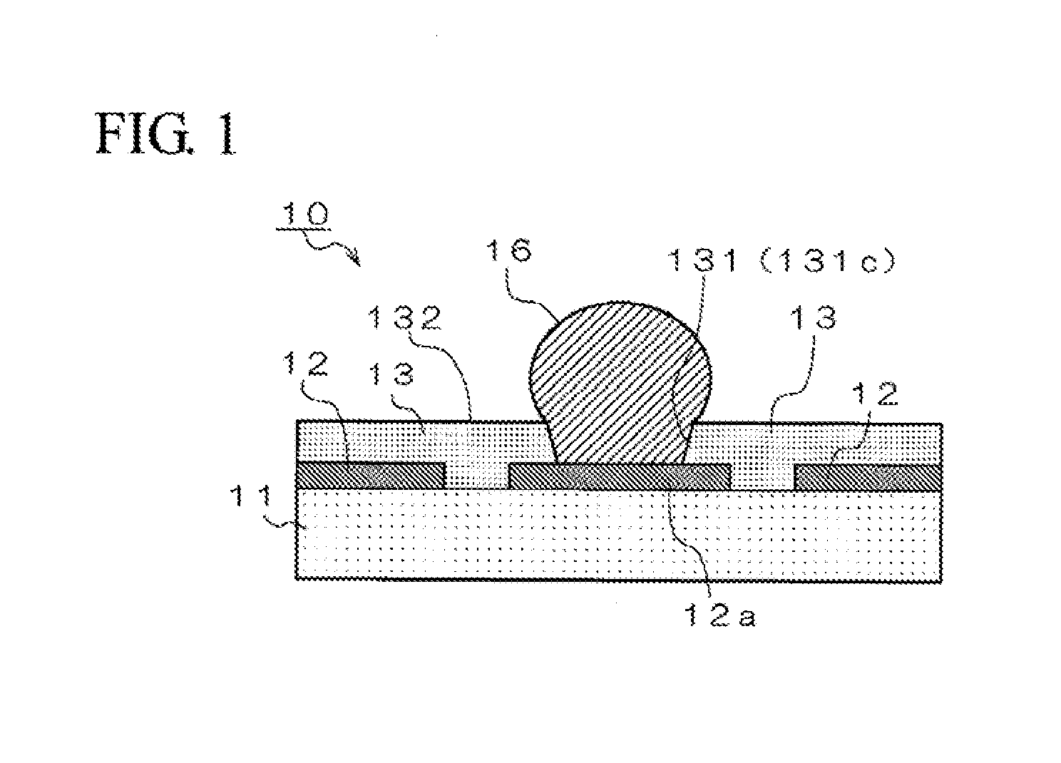
Figure 2 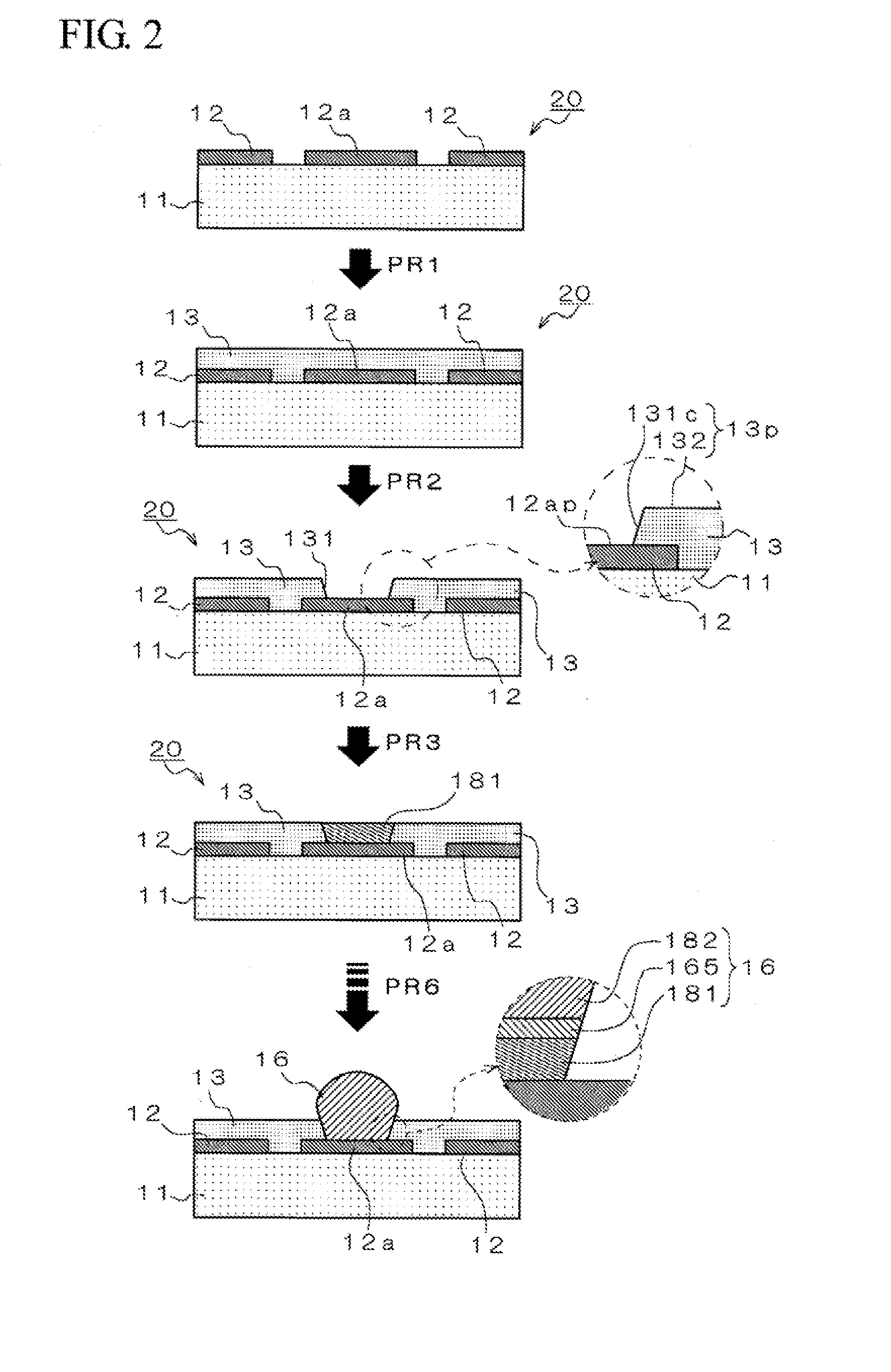
Figure 3
Abstract
Description
CROSS-REFERENCE TO RELATED APPLICATIONS
[0001] The present application claims priority from Japanese Patent Application No. 2010-279707, which was filed on Dec. 15, 2010, and Japanese Patent Application No. 2011-227310, which was filed on Oct. 14, 2011, the disclosure of which is herein incorporated by reference in its entirety.BACKGROUND OF THE INVENTION
[0002] 1. Field of the Invention
[0003] The present invention relates to a wiring board and a method of manufacturing the same. In more detail, embodiments of the present invention relate to wiring boards having a conductor post and methods of manufacturing such wiring boards.
[0004] 2. Description of Related Art
[0005] In recent years, as a high-density packaging technique, for example, a C4 (controlled collapse chip connection) method has been adopted. Wiring boards utilized in C4 methods have a surface that is covered by a solder resist layer, and wherein a bump (conductor post) is vertically arranged, in an optionally bored opening in th...
Examples
embodiment
[0136]a wiring board 10 of the invention is more specifically described below with respect to the following Embodiment, but it should not be construed that the invention is limited to this Embodiment.
[0137](1) Wiring Board 10:
[0138]A wiring substrate 10 (see FIG. 1) manufactured according to this Embodiment includes a conductor layer 12 laminated on the side of one surface of a core substrate 11, a solder resist layer 13 laminated on this conductor layer 12, and a conductor post 16 to be electrically connected to a conductor layer 12a which is disposed in a lower portion of a through-hole 131 provided in the solder resist layer 13. The core substrate 11 is composed of glass epoxy (epoxy resin containing glass fibers as a core material) having a thickness of 0.8 mm. Also, the conductor layer 12 is one obtained by patterning a copper foil having a thickness of 12 μm on one surface of the core substrate 11. Furthermore, the solder resist layer 13 has a thickness of 21 μm and contains a...