
Stacked package, method of fabricating stacked package, and method of mounting stacked package fabricated by the method
a technology of stacked packages and fabricated methods, which is applied in the direction of electrical equipment, semiconductor devices, semiconductor/solid-state device details, etc., can solve the problems of serious warpage of a substrate, undesirable warpage of various substrates, etc., and achieves the effect of suppressing warpage, minimizing load applied to the package, and being convenient to fabrica
Patent Information
- Authority / Receiving Office
- US · United States
- Current Assignee / Owner
- Publication Date
- 2012-10-04
Smart Images
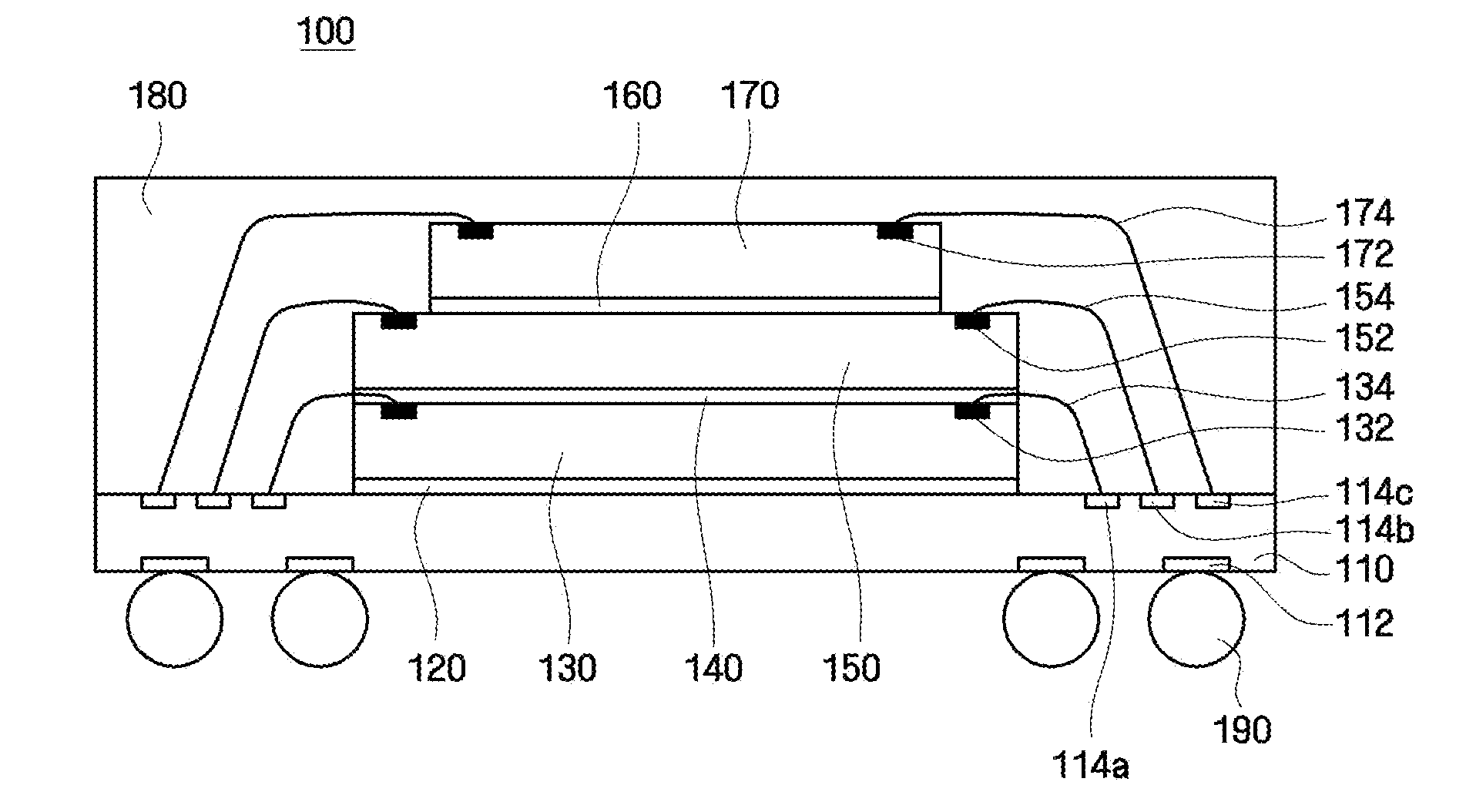
Figure 1 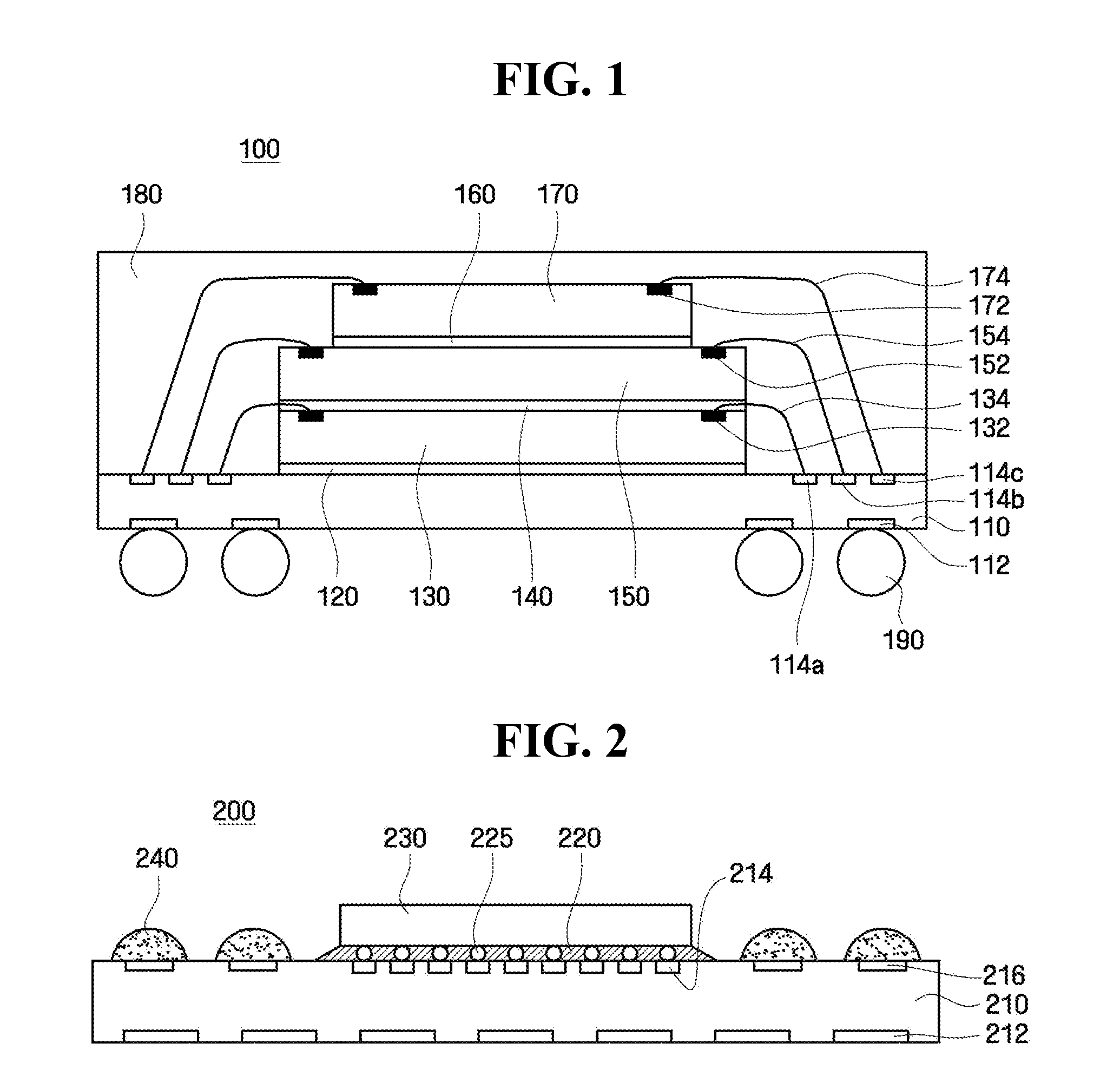
Figure 2 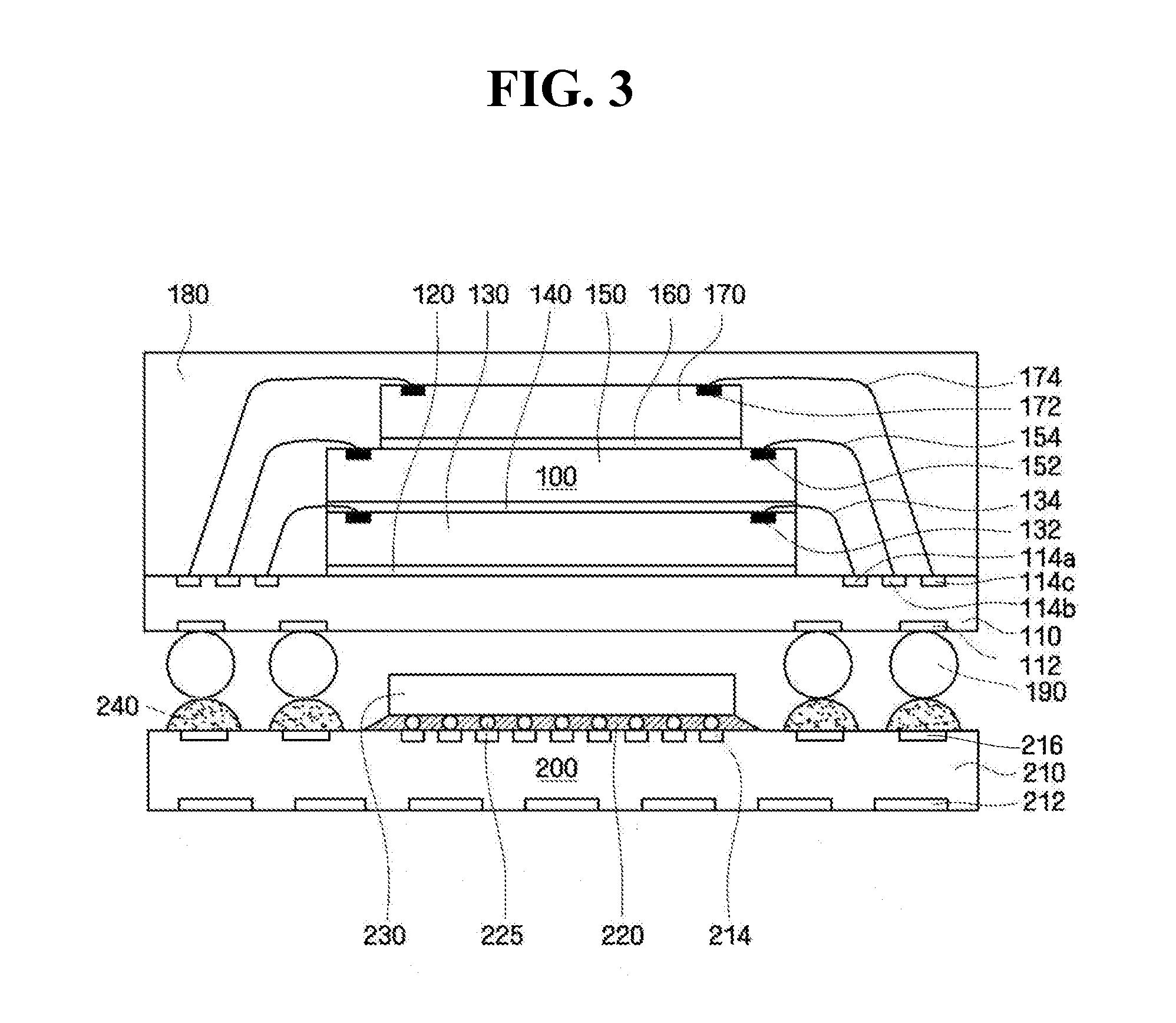
Figure 3
Abstract
Description
CROSS-REFERENCE TO RELATED APPLICATION
[0001] This application claims priority from Korean Patent Application No. 10-2010-0119762 filed on Nov. 29, 2010 in the Korean Intellectual Property Office, and all the benefits accruing therefrom under 35 U.S.C. 119, the contents of which in its entirety are herein incorporated by reference.BACKGROUND
[0002] 1. Field
[0003] The present disclosure relates to a stacked package, a method of fabricating a stacked package, and a method of mounting the stacked package fabricated by the same.
[0004] 2. Description of the Related Art
[0005] In recent years, as semiconductor device applications continue to demand ever higher performance, certain semiconductor chip sizes and package sizes are increasing. With the trend of electronic devices toward slimness, a thickness of a printed circuit board (PCB) on which packages are mounted often needs to be reduced. As a result, when semiconductor packages are mounted on the PCB, a serious warpage of a substrate may be c...
Examples
Embodiment Construction
[0019]The present disclosure will now be described more fully hereinafter with reference to the accompanying drawings, in which certain embodiments are shown. This invention may, however, be embodied in different forms and should not be construed as limited to the embodiments set forth herein. In the attached figures, the thickness of layers and regions is exaggerated for clarity.
[0020]It will also be understood that when a layer is referred to as being “on” another layer or substrate, it can be directly on the other layer or substrate, or intervening layers may also be present. In contrast, when an element is referred to as being “directly on” another element, there are no intervening elements present.
[0021]Spatially relative terms, such as “beneath,”“below,”“lower,”“above,”“upper” and the like, may be used herein for ease of description to describe one element or feature's relationship to another element(s) or feature(s) as illustrated in the figures. It will be understood that th...