
Conductive film, display device equipped with same, and method for determining pattern of conductive film
Patent Information
- Authority / Receiving Office
- US · United States
- Current Assignee / Owner
- Publication Date
- 2015-01-15
Smart Images
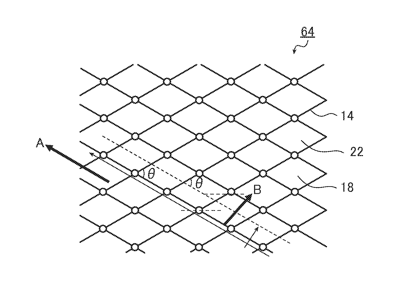
Figure 1 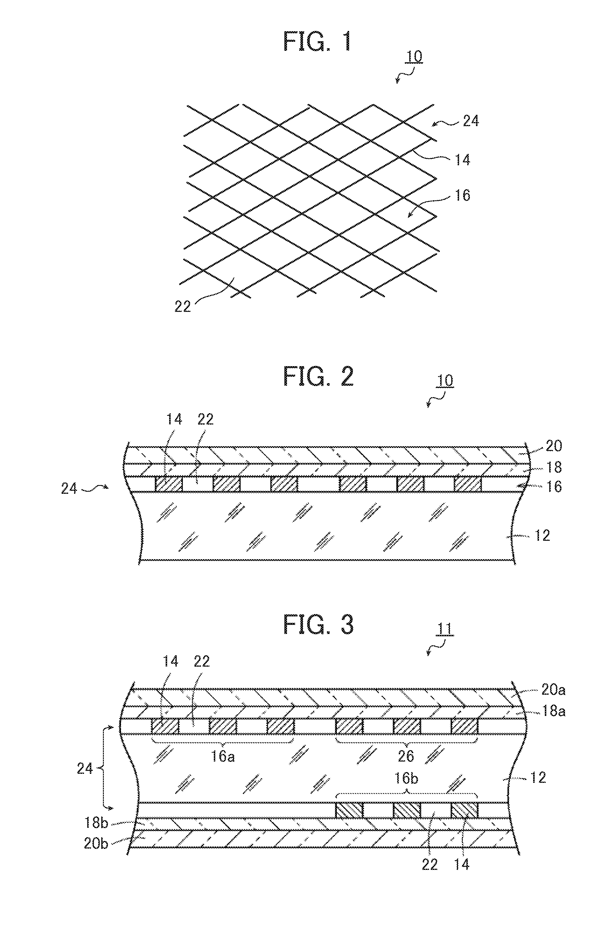
Figure 2 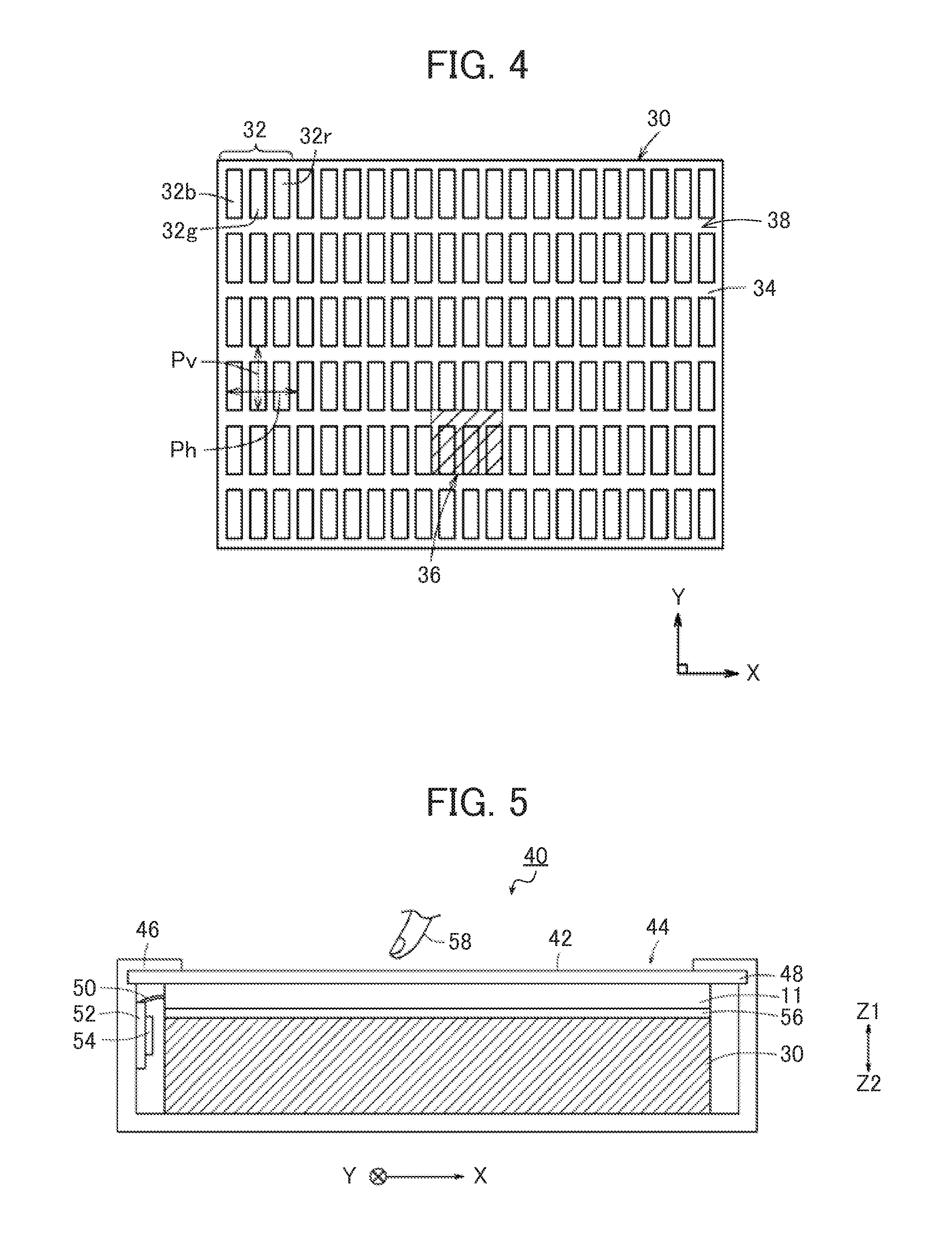
Figure 3
Abstract
Description
CROSS-REFERENCE TO RELATED APPLICATIONS
[0001] This application is a continuation of International Application No. PCT / JP2013 / 055287 filed on Feb. 28, 2013, which claims priority under 35 U.S.C. §119(a) to Japanese Patent Application No. 2012-082706 filed on Mar. 30, 2012. Each of the above applications is hereby expressly incorporated by reference, in its entirety, into the present application.BACKGROUND OF THE INVENTION
[0002] The present invention relates to a conductive film, a display device equipped with the conductive film, and a method for determining a pattern of the conductive film.
[0003] Examples of a conductive film installed on a display unit of a display device (hereinafter also referred to as “display”) include a conductive film for electromagnetic shields and a conductive film for touch panels (for example, see JP 2009-117683 A and JP 2011-216379 A).
[0004] JP 2009-117683 A, a published patent application filed by the same applicant as the present application, discloses tha...
Examples
examples
[0137]Hereinafter, the present invention will be described in more detail with reference to examples of the present invention.
[0138]A wiring pattern 24 was prepared by giving irregularity to the optimized rhomboidal wiring pattern 64 illustrated in FIG. 14, and the resultant wiring pattern was superimposed on the BM pattern 38 illustrated in FIG. 7A so as to conduct sensory evaluation about the visibility of moire.
[0139]In the optimized rhomboidal wiring patterns 64 illustrated in FIG. 14, the angle of rhomboid is 30° and the pitch of rhomboid is 200 μm. The thin metal wires 14 as used were two in type of line width, those with a line width of 2 μm and those with a line width of 4 μm.
[0140]A black matrix (168 v8 h32) having the BM pattern 38 illustrated in FIG. 7A was used as the BM 34.
[0141]First, as Example 1, two types of wiring patterns, namely, a pitch-preserved wiring pattern (pitch preserved) in which the width of the thin metal wires 14 was 4 the angle of rhomboid was 30°, t...