
Energy conversion cells using tapered waveguide spectral splitters
a technology of energy conversion cells and spectral splitters, which is applied in the field of cells, can solve the problems of affecting the efficiency of energy conversion cells, and requiring kinetic energy for machines, etc., and achieves the effects of easy manufacturing, increased energy efficiency of radiant energy conversion cells, and low cos
Patent Information
- Authority / Receiving Office
- US · United States
- Current Assignee / Owner
- Publication Date
- 2015-08-20
Smart Images
Figure 1 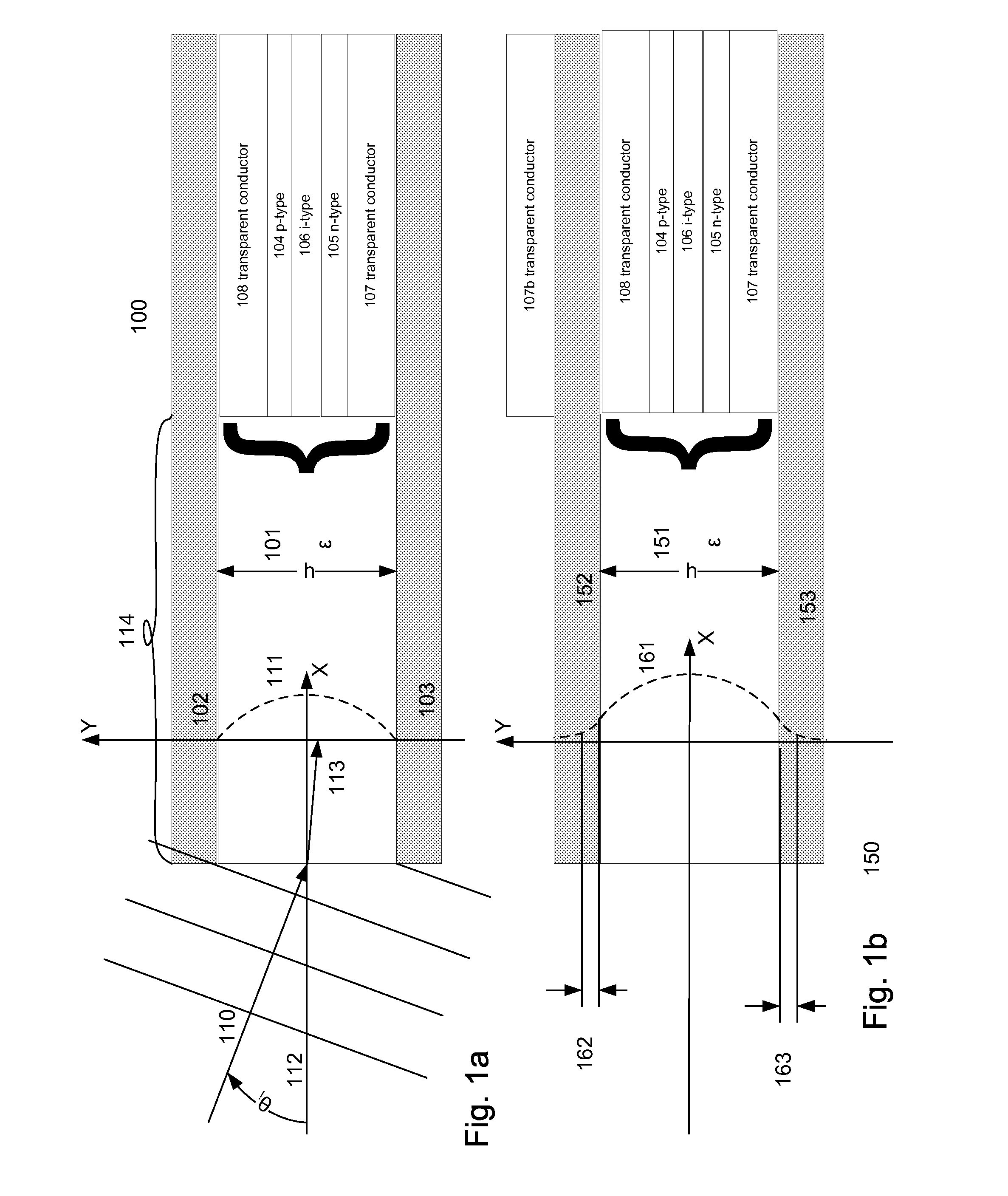
Figure 2 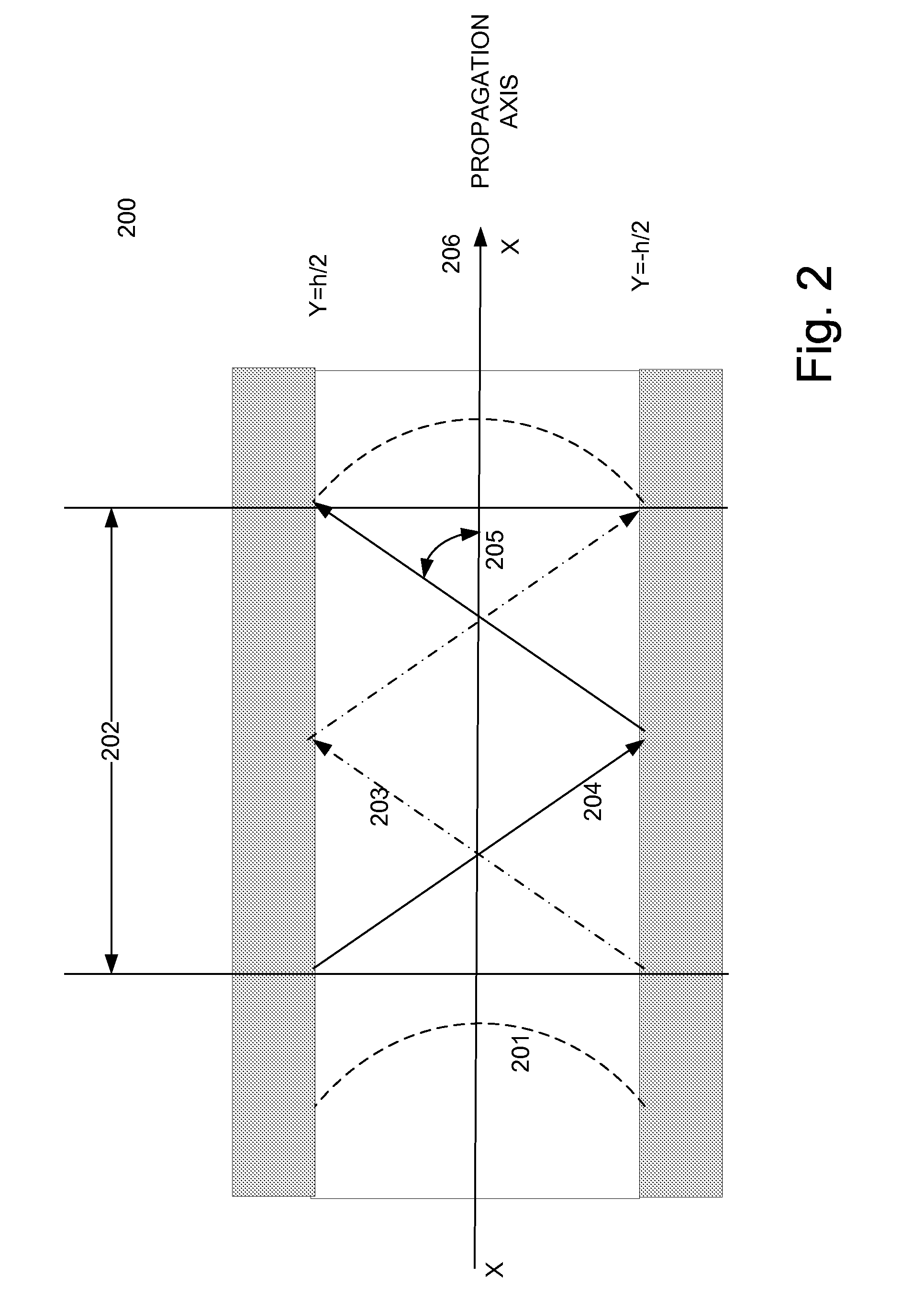
Figure 3
Abstract
Description
RELATED APPLICATIONS
[0001] Aspects of the present invention were first disclosed in U.S. Patent Application 61 / 701,687 to Andle and Wertsberger, entitled “Continuous Resonant Trap Refractor, Waveguide Based Energy Transducers, Energy Conversion Cells, and Display Panels Using Same”, filed 16 Sep. 2012. Further refinements of the tapered waveguide based Continuous Resonant Trap Refractor (CRTR) and to lateral waveguides with which CRTRs may cooperate, were disclosed together with various practical applications thereof in the following additional U.S. Patent Applications: 61 / 713,602, entitled “Image Array Sensor”, filed 14 Oct. 2012; 61 / 718,181, entitled “Nano-Scale Continuous Resonance Trap Refractor”, filed 24 Oct. 2012; 61 / 723,832, entitled “Pixel Structure Using Tapered Light Waveguides, Displays, Display Panels, and Devices Using Same”, filed 8 Nov. 2012; 61 / 723,773, entitled “Optical Structure for Banknote Authentication”, filed 7 Nov. 2012; Ser. No. 13 / 726,044 entitled “Pixel St...
Examples
Embodiment Construction
[0071]Certain figures and embodiments of the invention will be described herein by way of example to increase the understanding of different aspects of the invention.
[0072]FIGS. 1a and 1b alternately depict a short region of waveguide with insignificant variation of thickness, and are provided for simple explanation of the propagation characteristics of radiant energy within such waveguides. For the purpose of explanation, FIGS. 1a and 1b may be considered to represent a cutout of a short region of the CRTR tapered core waveguide.
[0073]FIG. 1.a shows a two dimensional waveguide 100 comprising a waveguide core material 101 of thickness (width), h, formed between conductors 102 and 103. Optionally, the waveguide core material 101 could be replaced by a plurality of layers forming an aggregate optically equivalent to a uniform material having dielectric constant, E, and the same overall thickness. Such construction would be recognized as equivalent by the skilled artisan. In plurality ...