
Micro-transfer-printed compound sensor device
a sensor device and microtransfer technology, applied in microstructural technology, microstructure technology, precision positioning equipment, etc., can solve the problems of less efficiency, not more efficiently integrating processing and sensing devices, and not well suited
Patent Information
- Authority / Receiving Office
- US · United States
- Patent Type
- Applications(United States)
- Current Assignee / Owner
- Publication Date
- 2017-08-10
Smart Images
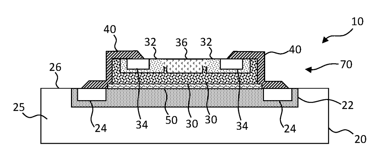
Figure 1 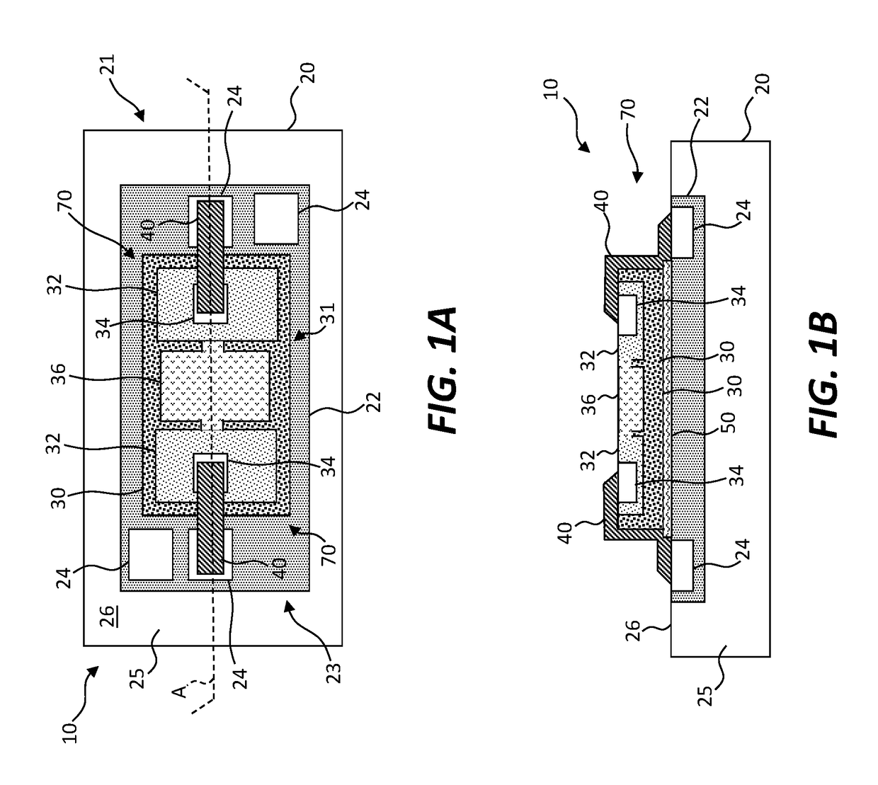
Figure 2 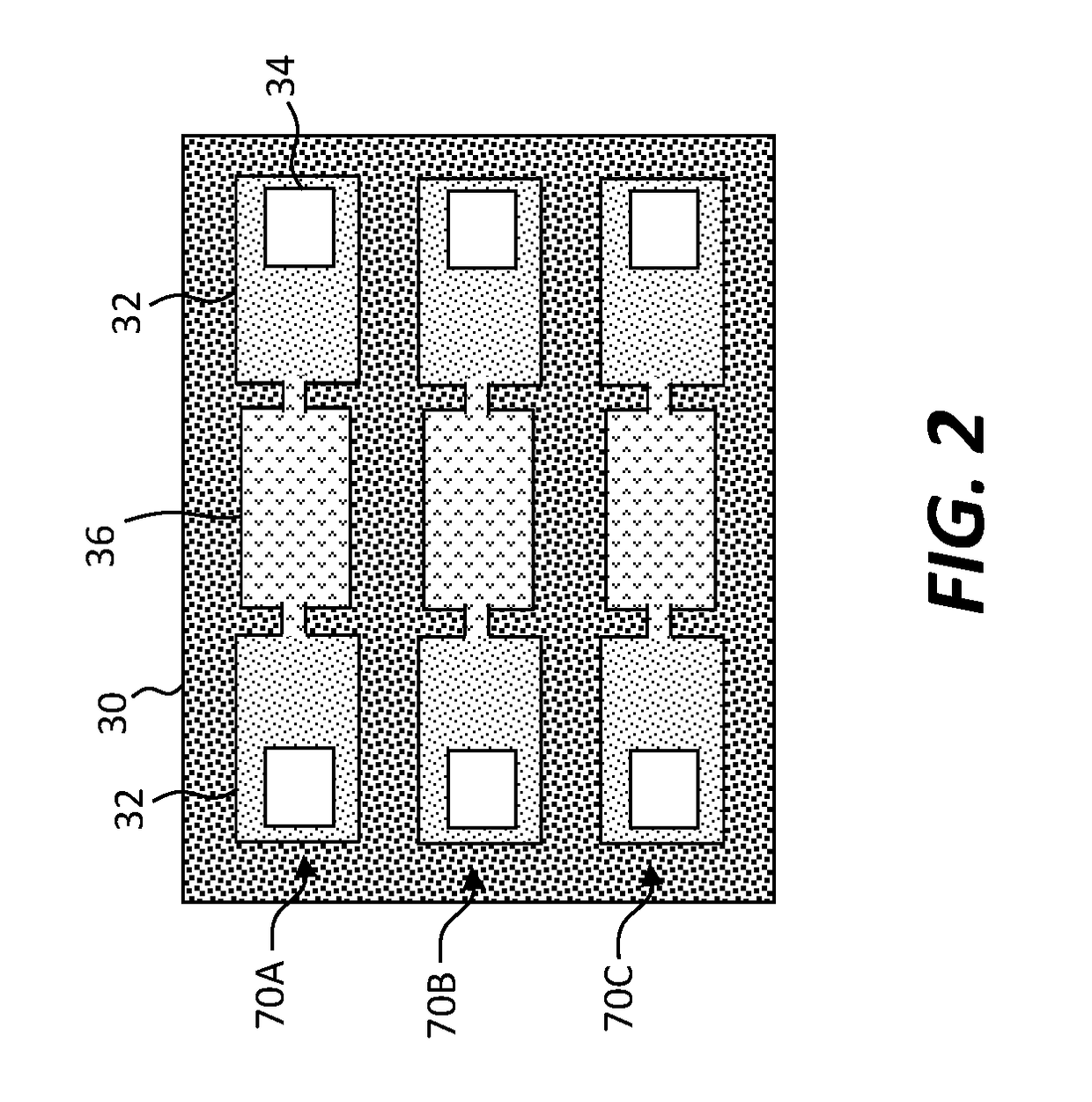
Figure 3
Abstract
Description
PRIORITY APPLICATIONS
[0001] This application claims priority to U.S. Provisional Patent Application No. 62 / 291,830, filed Feb. 5, 2016, entitled Micro-Transfer-Printed Compound Sensor Device, and to U.S. Provisional Patent Application No. 62 / 293,612, filed Feb. 10, 2016, entitled Micro-Transfer-Printed Compound Sensor Device, the contents of all of which are hereby incorporated by reference in their entirety.CROSS REFERENCE TO RELATED APPLICATION
[0002] This application is related to U.S. patent application Ser. No. 15 / 047,250 filed Feb. 18, 2016, entitled Micro-Transfer-Printed Acoustic Wave Filter Device, and to U.S. patent application Ser. No. 15 / 048,134, filed Feb. 19, 2016, entitled Compound Micro-Transfer-Printed Optical Filter Device, and to G.B. patent application Ser. No. 1419515.0 filed Nov. 3, 2014, entitled Magnetic Field Sensor and Method of Making Same, the contents of all of which are hereby incorporated by reference in their entirety.FIELD OF THE INVENTION
[0003] The pres...
Examples
Embodiment Construction
[0069]Referring to the schematic plan view of FIG. 1A and the schematic cross section of FIG. 1B taken across cross section line A of FIG. 1A, in an embodiment of the present invention, a compound sensor device 10 includes a semiconductor substrate 20. An active electronic circuit 22 is formed in or on the semiconductor substrate 20, for example, using photolithographic methods found in the integrated circuit industry. The active electronic circuit 22 can be, for example, a circuit for controlling a sensor 70, sending or receiving signals to or from the sensor 70, or processing signals received from the sensor 70. The active electronic circuit 22 can also send and receive signals to and from an external device (not shown). The active electronic circuit 22 includes two or more circuit connection pads 24 connected to the active electronic circuit 22 for providing signals to the active electronic circuit 22 or receiving signals from the active electronic circuit 22. The sensor 70 is re...