
Organic light emitting diode display panel and manufacturing method thereof
Patent Information
- Authority / Receiving Office
- US · United States
- Current Assignee / Owner
- Publication Date
- 2020-03-19
Smart Images
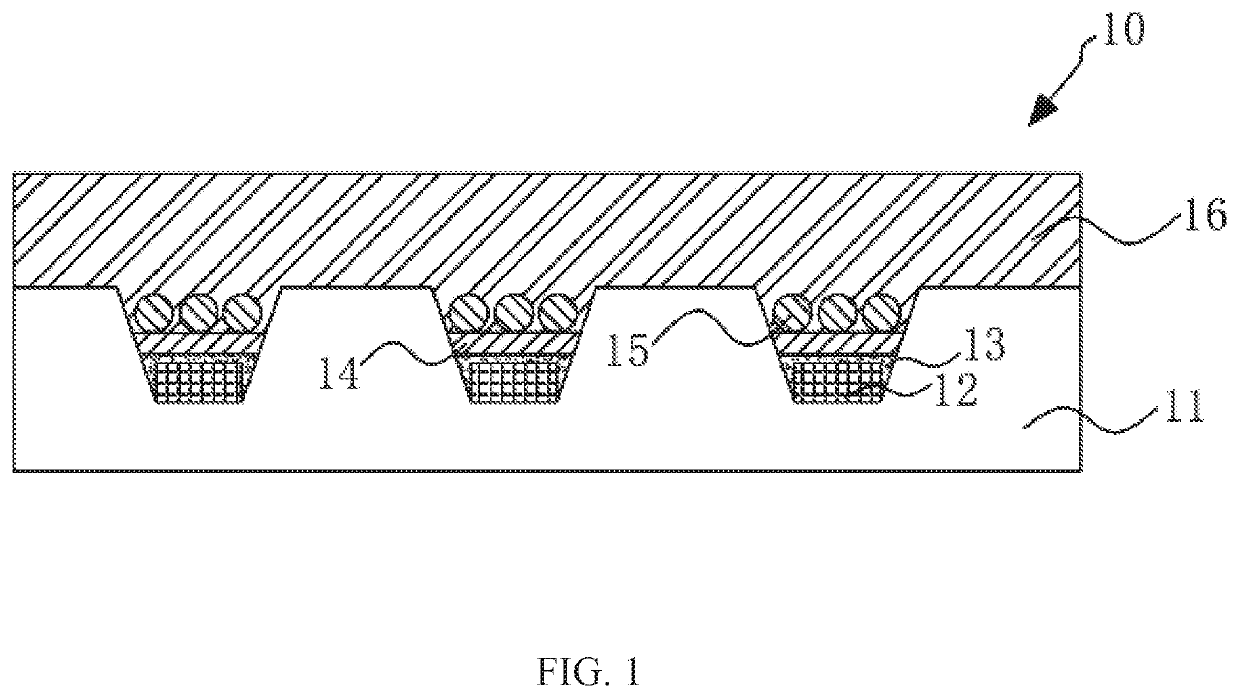
Figure 1 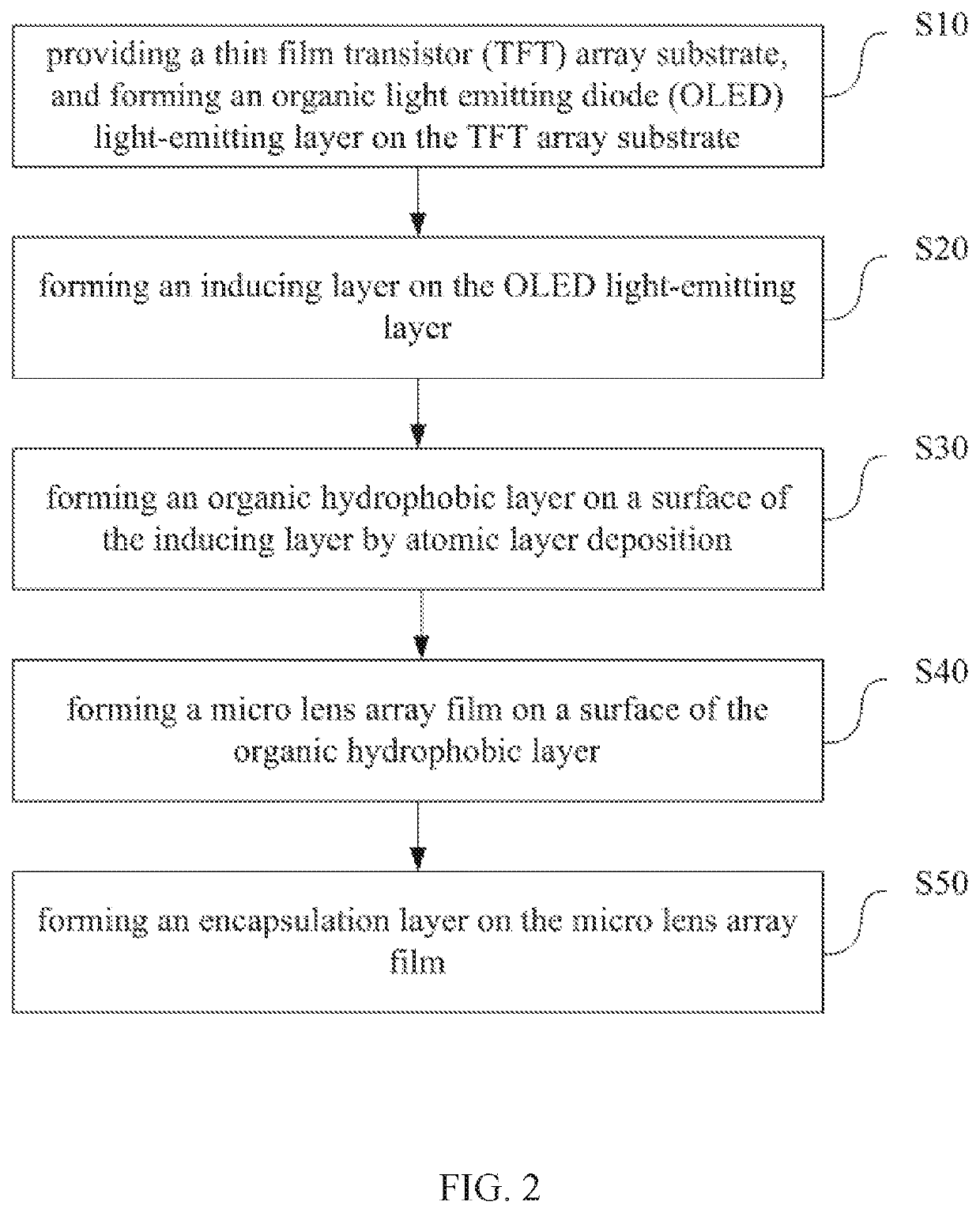
Figure 2 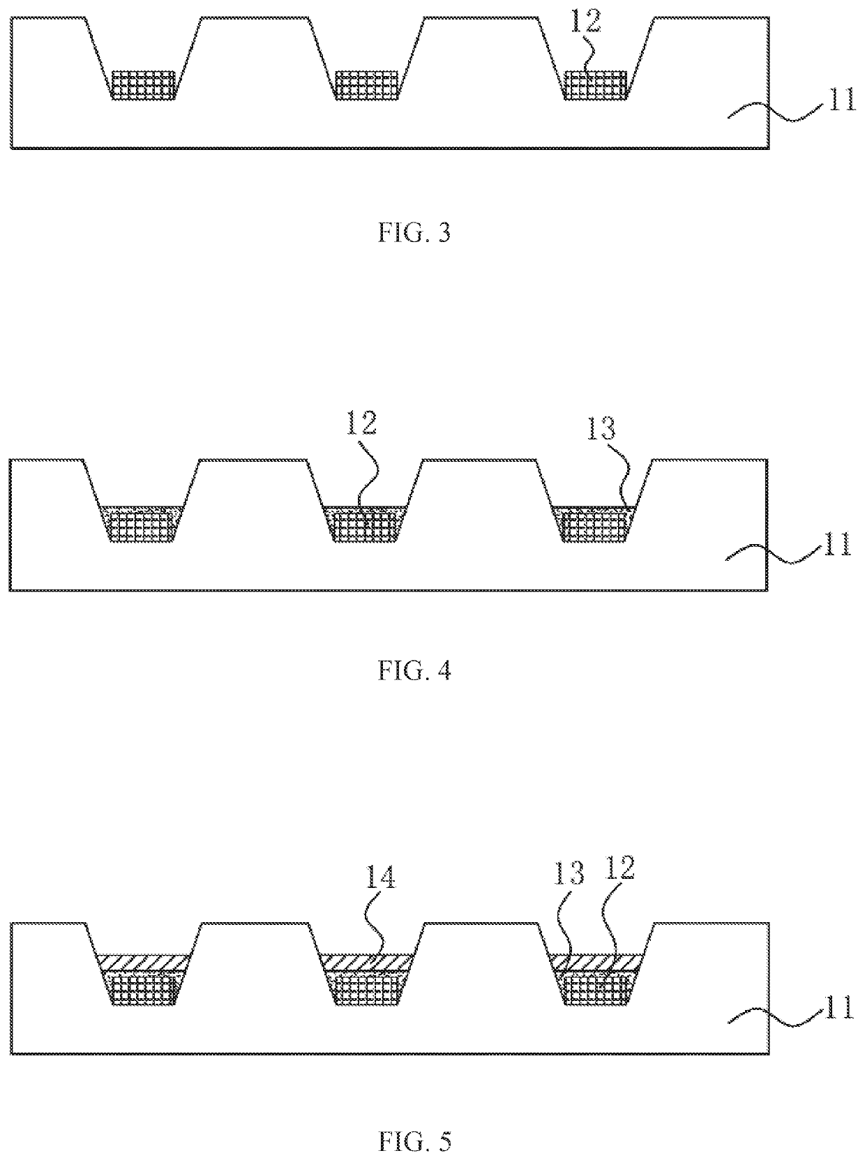
Figure 3
Abstract
Description
FIELD OF DISCLOSURE
[0001] The present disclosure relates to the field of display technologies, and more particularly to an organic light emitting diode (OLED) display device and a manufacturing method thereof.BACKGROUND
[0002] OLED devices have advantages of being light weight, wide viewing angles, fast response times, low temperature resistance, high luminous efficiency, etc., and have received extensive attention in the display field. Especially, OLEDs can be made into flexible displays on flexible substrates, making OLEDs having a broader application prospect. However, light-emitting efficiency of OLED devices is still low, so how to effectively improve the light-emitting efficiency of OLED devices is still a difficult challenge.
[0003] Related researches have shown that doping an appropriate amount of small-sized transparent particles in the light penetrating film layer can improve light-emitting efficiency of the film layer. A micro lens technology currently under study is based on ...
Examples
Embodiment Construction
[0035]The following embodiments refer to the accompanying drawings for exemplifying specific implementable embodiments of the present disclosure. Moreover, directional terms described by the present disclosure, such as upper, lower, front, back, left, right, inner, outer, side, etc., are only directions by referring to the accompanying drawings, and thus the used directional terms are used to describe and understand the present disclosure, but the present disclosure is not limited thereto. In the drawings, the same reference symbol represents the same or similar components.
[0036]The invention is directed to an existing OLED display panel. Since a micro lens structure is arranged on an OLED device, the micro lens is usually prepared by using ink jet printing technology, and ink droplets have a relatively large polarity and are printed on a surface of the film with a small contact angle. The surface of the film is easily wetted, which causes the luminous efficiency of the obtained mic...