
Photosensor system and drive control method thereof
a technology of drive control and photosensor, which is applied in the field of photosensor systems, can solve the problems of reducing the reliability of the photosensor, affecting the reliability of the image reading apparatus, and inevitably changing the effective voltage applied to each gate terminal, and achieving the effect of high reliability and change in the sensitivity characteristi
Patent Information
- Authority / Receiving Office
- US · United States
- Patent Type
- Patents(United States)
- Current Assignee / Owner
- Publication Date
- 2005-05-03
- Estimated Expiration
- Not applicable · inactive patent
Smart Images
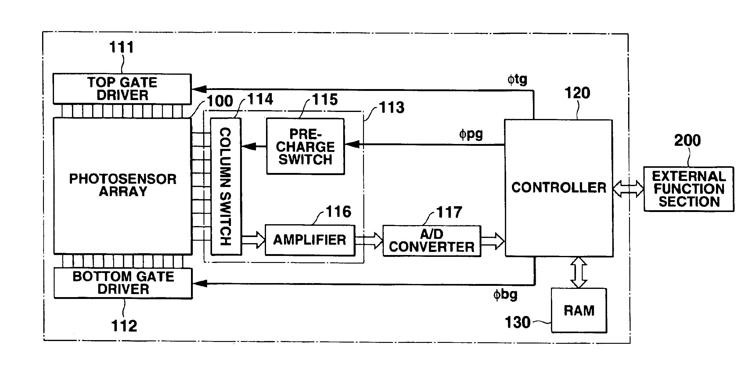
Figure 1 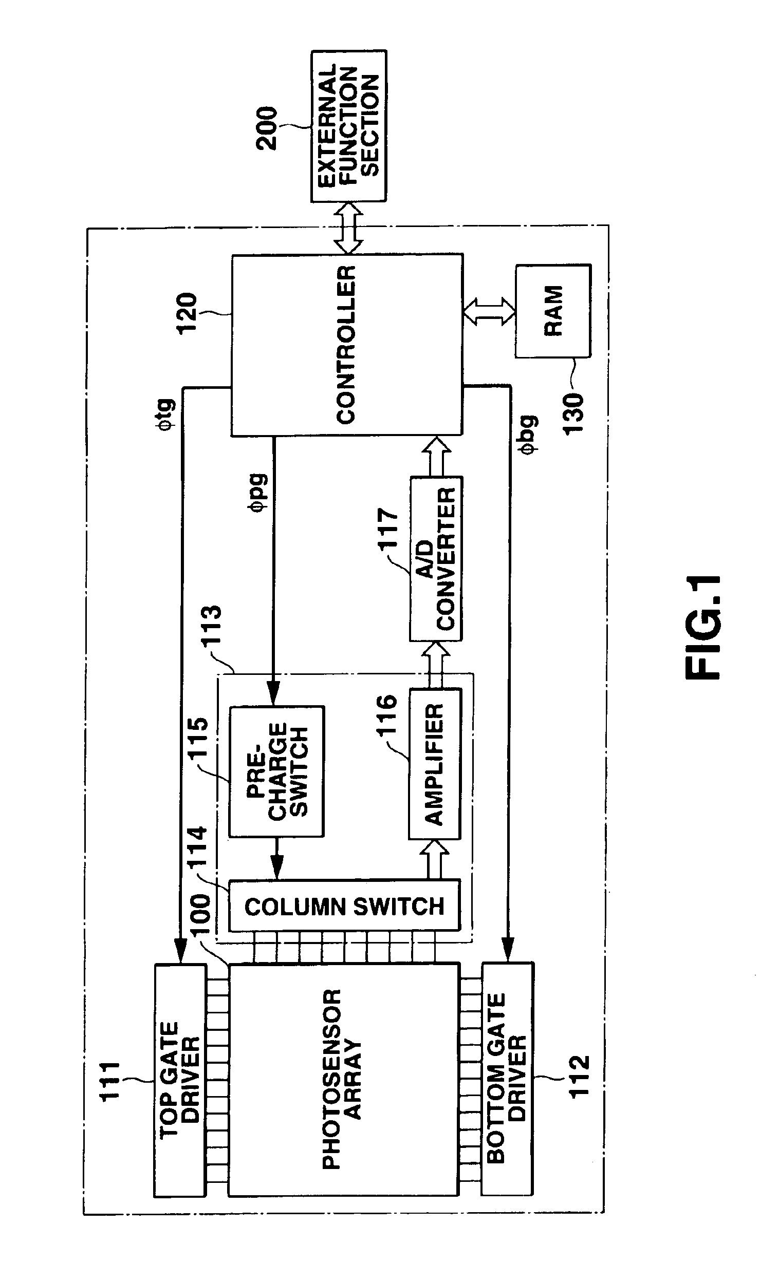
Figure 2 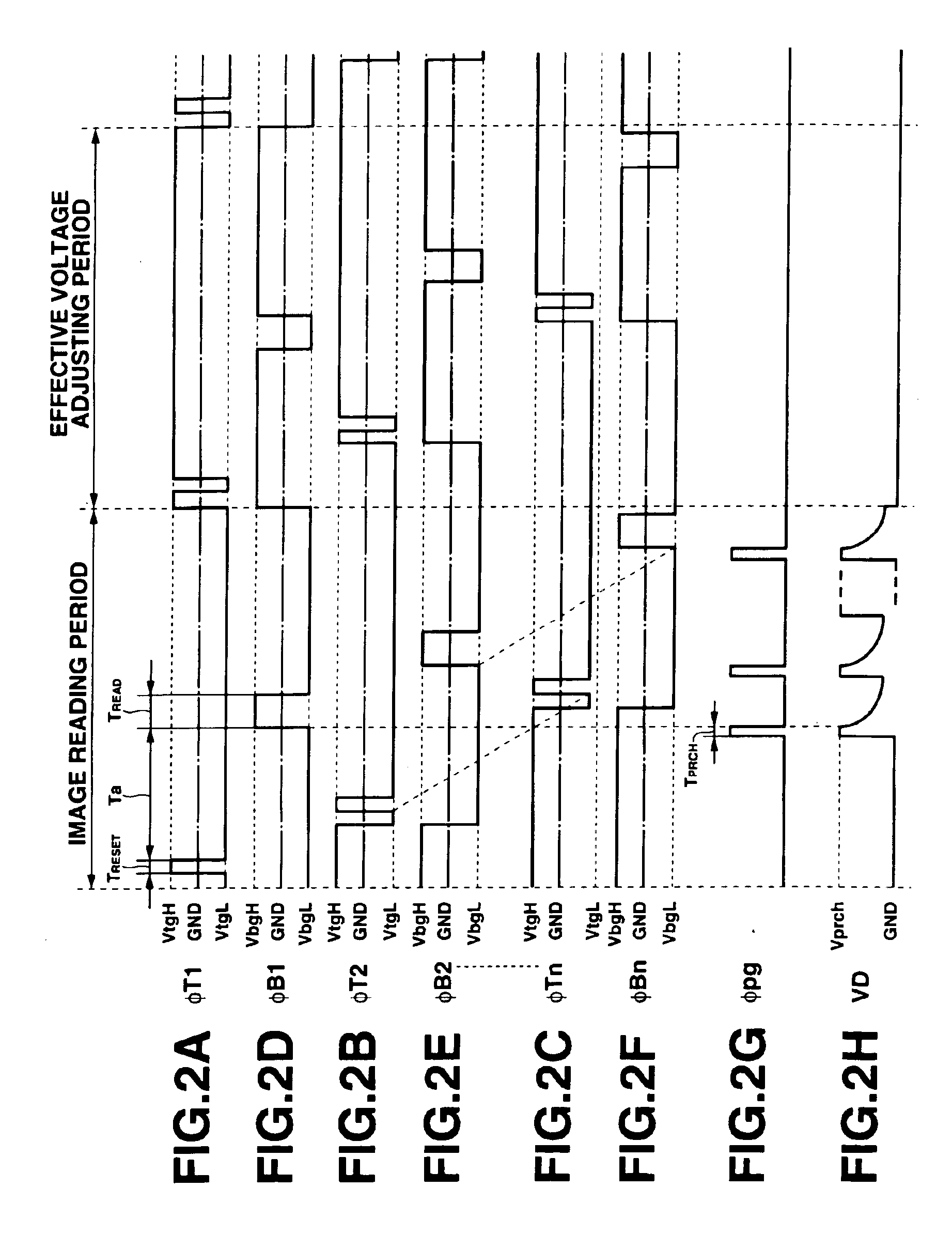
Figure 3
Abstract
Description
CROSS-REFERENCE TO RELATED APPLICATIONS
[0001] This application is based upon and claims the benefit of priority from the prior Japanese Patent Applications No. 11-271882, filed Sep. 27, 1999; and No. 11-370533, filed Dec. 27, 1999, the entire contents of which are incorporated herein by reference.BACKGROUND OF THE INVENTION
[0002] This invention relates to a photosensor system having a two-dimensionally arranged photosensor array, and a method for drive-controlling the system.
[0003] Imaging apparatuses such as electronic still cameras, video cameras, etc. have come to be very widely used. These imaging apparatuses employ a solid-state imaging device, such as a CCD (Charge Coupled Device), which serves as a photoelectric converting device for converting an image of a to-be-photographed subject into an image signal. As well known, the CCD has a structure in which photosensors (light receiving elements) such as photodiodes, or thin film transistors (TFT: Thin Film Transistor) are arranged ...
Examples
second embodiment
[0069]A method for controlling a photosensitive system according to the invention will be described with reference to FIGS. 4A-5B.
first embodiment
[0070]This embodiment differs from the first embodiment in that, in the former, the reset pulse signal and the readout pulse signal used in the image reading period each have a high level voltage and a low level voltage which are asymmetrical with respect to the GND level (0 V).
[0071]FIGS. 4A-4H are timing charts illustrating operation timing at each row employed in the photosensor system control method of the second embodiment of the invention. FIGS. 5A and 5B are timing charts illustrating in detail the waveforms of the voltage signals applied to the top and bottom gate terminals TG and BG of each double-gate photosensor 10 in this embodiment. The same control as employed in the above-described first embodiment will not be described in detail.
[0072]In the control method of this embodiment, at first, reset pulse signals φT1, φT2, . . . φTn shown in FIGS. 4A-4C are sequentially applied to the top gate lines 101, thereby sequentially starting reset periods Treset for respective rows,...
third embodiment
[0078]A method for controlling a photosensitive system according to the invention will be described with reference to FIGS. 6A-7B.
[0079]This embodiment is directed to a case similar to the second embodiment, where the reset pulse signal and the readout pulse signal used in the image reading period each have a high level voltage and a low level voltage which are asymmetrical with respect to the GND level (0 V).
[0080]FIGS. 6A-6H are timing charts illustrating operation timing at each row employed in the photosensor system control method of the third embodiment of the invention. FIGS. 7A and 7B are timing charts illustrating in detail the waveforms of the voltage signals applied to the top and bottom gate terminals TG and BG of each double-gate photosensor 10 in this embodiment. The same control as employed in the above-described embodiments will not be described in detail.
[0081]In the control method of this embodiment, at first, reset pulse signals φT1, φT2, . . . φTn shown in FIGS. 6...