
Illumination arrangement
a technology of illumination and arrangement, which is applied in the direction of waveguides, lighting and heating apparatus, instruments, etc., can solve the problems of undesirable, high cost and undesirable, and achieve the effects of reducing engineering and manufacturing costs, cost effective, and convenient us
Patent Information
- Authority / Receiving Office
- US · United States
- Patent Type
- Patents(United States)
- Current Assignee / Owner
- Publication Date
- 2006-06-06
- Estimated Expiration
- Not applicable · inactive patent
Smart Images
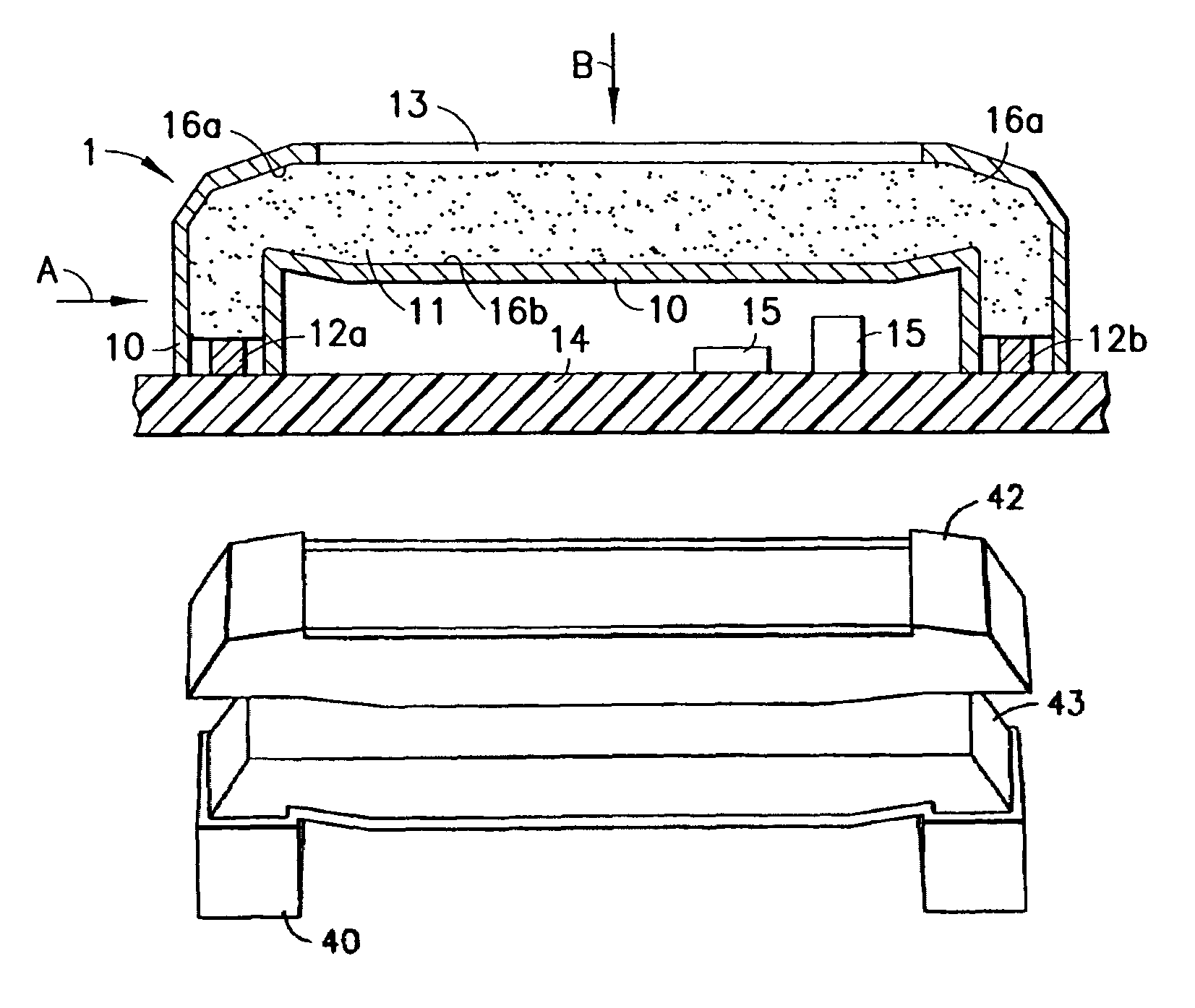
Figure 1 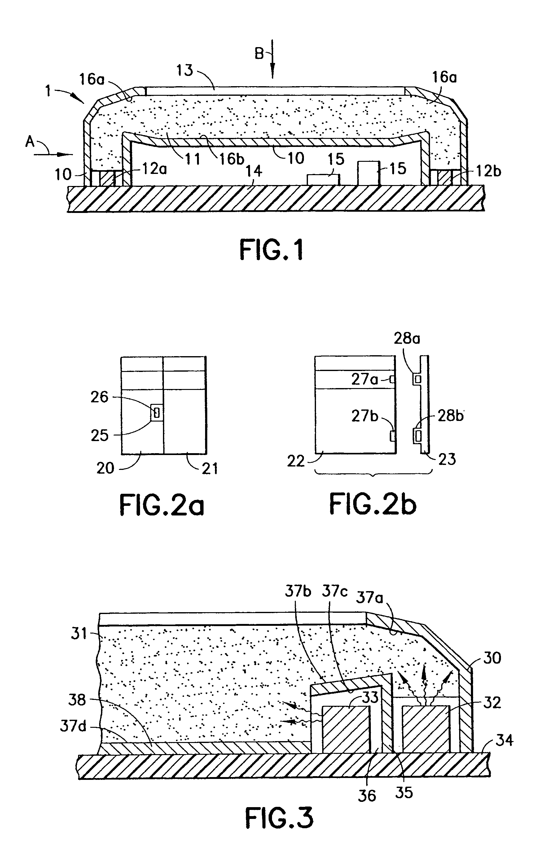
Figure 2 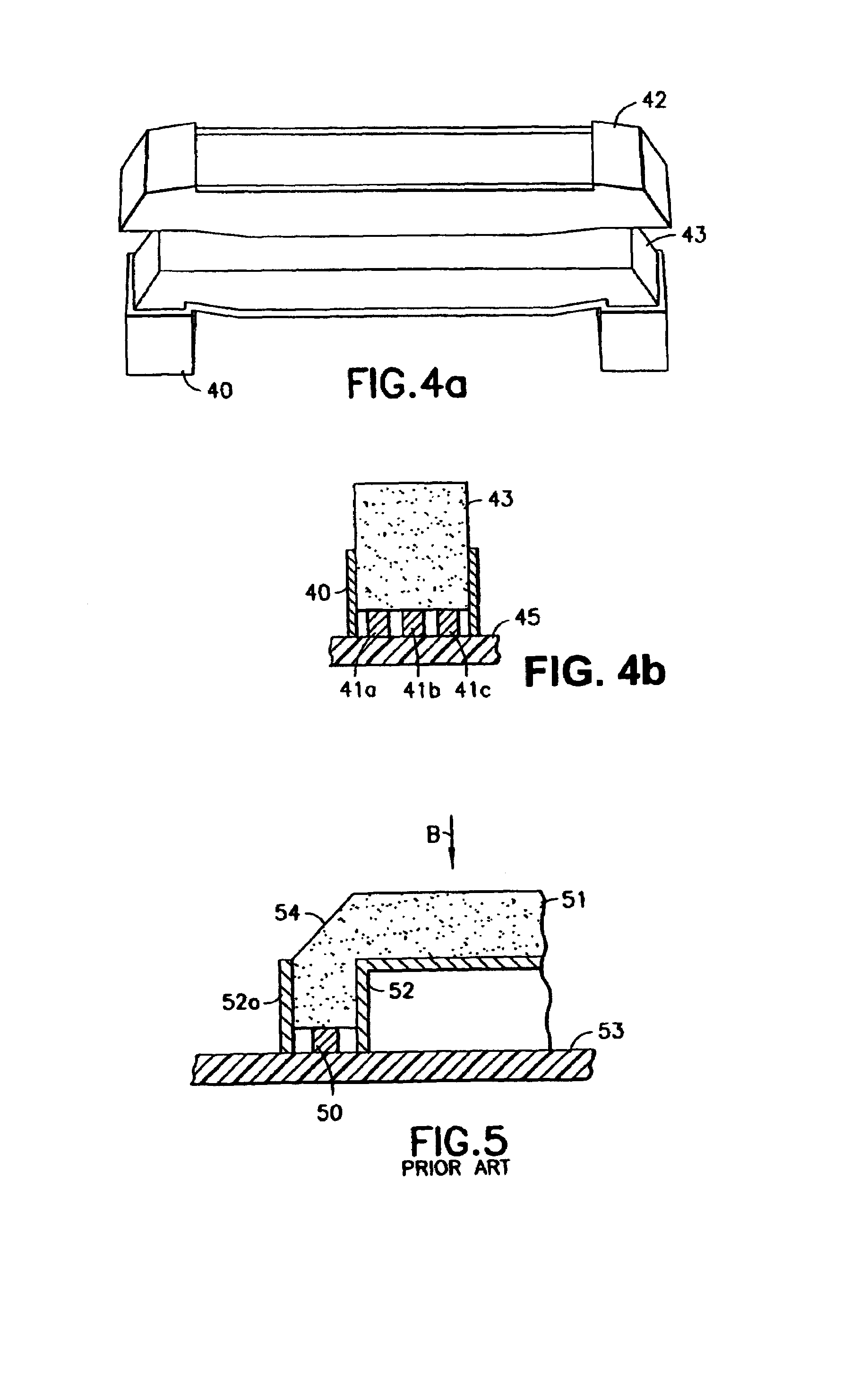
Figure 3
Abstract
Description
CROSS REFERENCE TO RELATED APPLICATIONS
[0001] This application claims priority to International Application No.: PCT / DE00 / 04270 which was published Jun. 7, 2001. This application further claims priority to German patent application 199957611.4 filed 30 Nov. 1999.TECHNICAL FIELD OF THE INVENTION
[0002] The invention relates generally to an illumination arrangement having an optical waveguide, a light source, coupled thereto, and a mount for the optical waveguide.BACKGROUND OF THE INVENTION
[0003] Known illumination arrangements wherein the light source comprises a light-emitting diode or a laser diode, is often used for general illumination or background illumination for liquid-crystal displays (LCD). Herein, the optical waveguide directs light, emitted by the coupled light source, out from the optical waveguide at a waveguide end or at a centrally located window. In the latter example, the surface of the optical waveguide is structured in the window region, e.g. by knobs, grooves, or by ...
Examples
Embodiment Construction
[0013]FIG. 1 shows an illumination arrangement 1 in a cross-sectional illustration. The arrangement comprises a mount 10 or an optical waveguide 11, into which one or more light sources 12a, 12b feed light. The light sources 12 are preferably light-emitting diodes (LED) or laser diodes, but other light sources such as incandescent lamps are also possible. The light source 12 and the mount 10 are mounted on a printed circuit board 14. The mount 10 surrounds the optical waveguide 11 in shell form in the regions in which the light has to be deflected and guided. In order to introduce the optical waveguide into the shell, and to be able to mount it, the mount 10 is formed from a plurality of shell elements. In the example of FIG. 1, the mount 10 contains on its top side a window 13 through which an observer B can observe the optical waveguide or the light can be coupled out. The window 13 in the mount 10 is configured in such a way that the illumination arrangement can serve as an eleme...