
Package for an integrated circuit
a technology for integrated circuits and packaging, applied in semiconductor devices, semiconductor/solid-state device details, electrical devices, etc., can solve the problems of composite construction carriers having a relatively small package footprint, no single piece-part alone providing adequate structural integrity, and consuming the smallest possible installed footprint of packaged devices, etc., to achieve small package footprint, small package footprint, and high degree of design flexibility
Patent Information
- Authority / Receiving Office
- US · United States
- Patent Type
- Patents(United States)
- Current Assignee / Owner
- Publication Date
- 2009-11-03
Smart Images
Figure 1 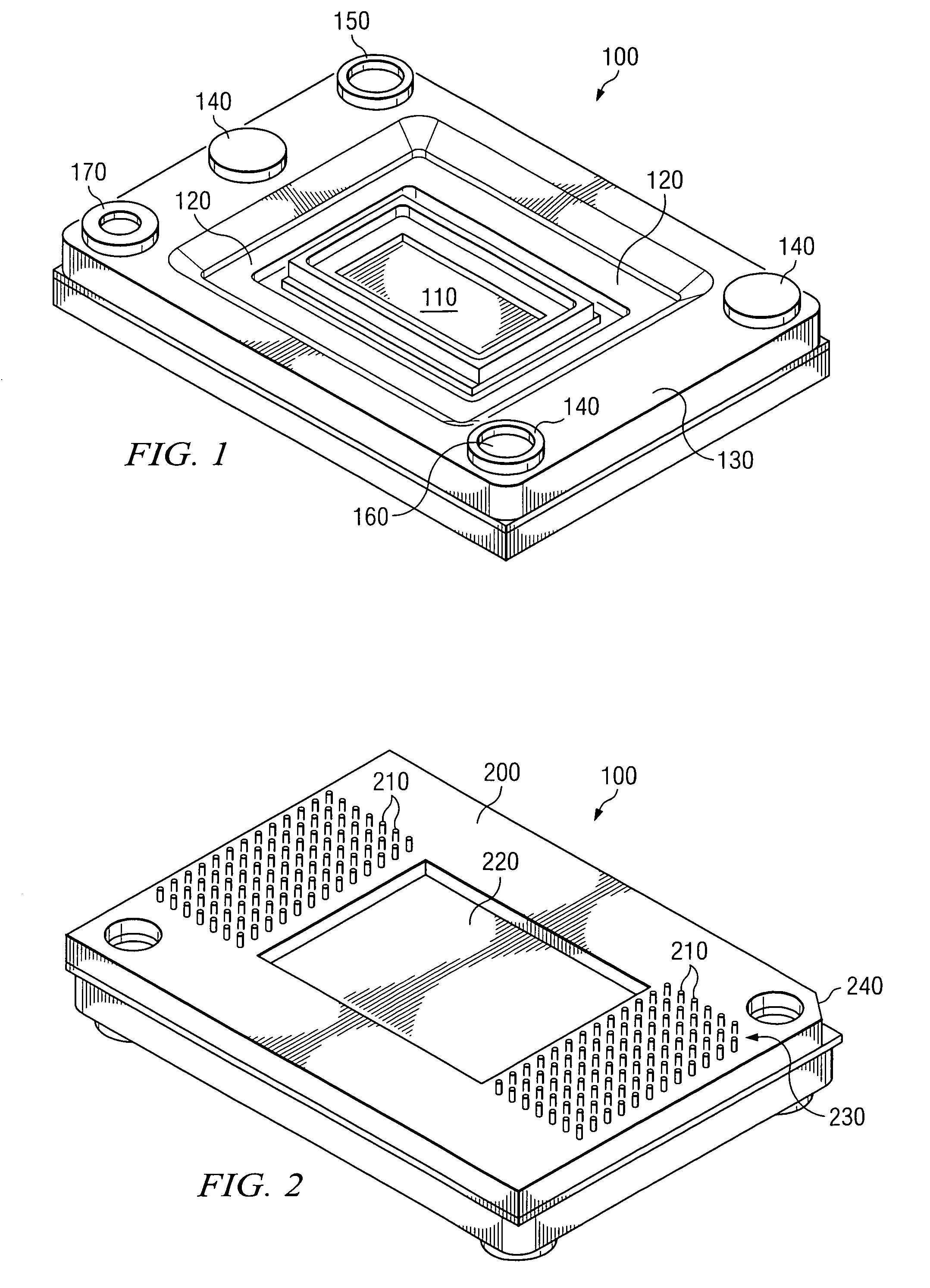
Figure 2 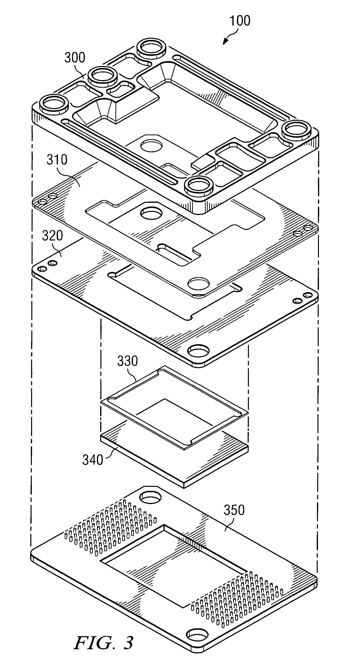
Figure 3
Abstract
Description
RELATED APPLICATIONS
[0001] This application is related to U.S. Provisional Patent Application Ser. No. 60 / 682,248 entitled “MONOLITHIC FRAME FOR A MEMS SPATIAL LIGHT MODULATOR IC,” which was filed on May 18, 2005.TECHNICAL FIELD OF THE INVENTION
[0002] This invention relates generally to the field of integrated circuit packaging and, more specifically, to a monolithic frame device for an integrated circuit (IC).BACKGROUND OF THE INVENTION
[0003] A package for a micro-electro-mechanical system (MEMS) spatial light modulator (SLM) integrated circuit (IC) is required to perform the functions of (1) furnishing an electrical connection between the integrated circuit (IC) and the system using the integrated circuit (IC), where the electrical connection must provide sufficient electrical signal integrity, (2) furnishing a thermal connection between the integrated circuit (IC) and the system using the integrated circuit (IC), where the thermal connection must provide a sufficiently low thermal r...
Examples
Embodiment Construction
[0026]Illustrative embodiments of the present invention are described in detail below. In the interest of clarity, not all features of an actual implementation are described in this specification. It will of course be appreciated that in the development of any such actual embodiment, numerous implementation-specific decisions must be made to achieve the developers' specific goals, such as compliance with system-related and business-related constraints, which will vary from one implementation to another. Moreover, it will be appreciated that such a development effort might be complex and time-consuming, but would nevertheless be a routine undertaking for those of ordinary skill in the art having the benefit of the present disclosure.
[0027]The present inventors have recognized several problems with respect to both composite construction carriers and principle-member construction carriers. As described above, composite construction strives to achieve sufficient structural integrity as ...