
Non-volatile memory device and method of fabricating the same
a memory device and non-volatile technology, applied in the field of semiconductor devices, can solve the problems of difficult selection of memory cells from each layer, difficulty in connecting memory cells in different layers, and high manufacturing cost, and achieve the effect of increasing integration
Patent Information
- Authority / Receiving Office
- US · United States
- Patent Type
- Patents(United States)
- Current Assignee / Owner
- Publication Date
- 2011-03-22
Smart Images
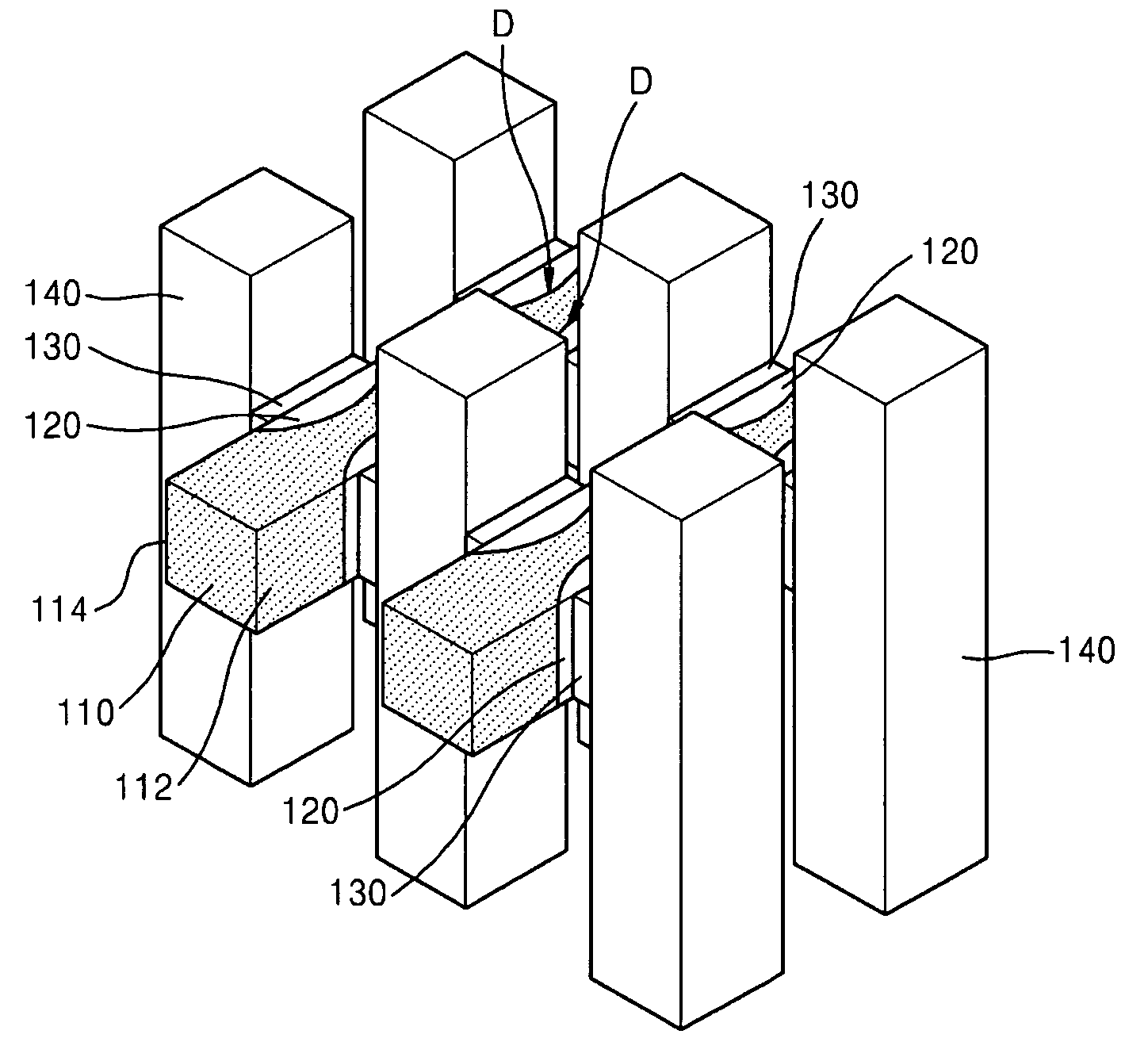
Figure 1 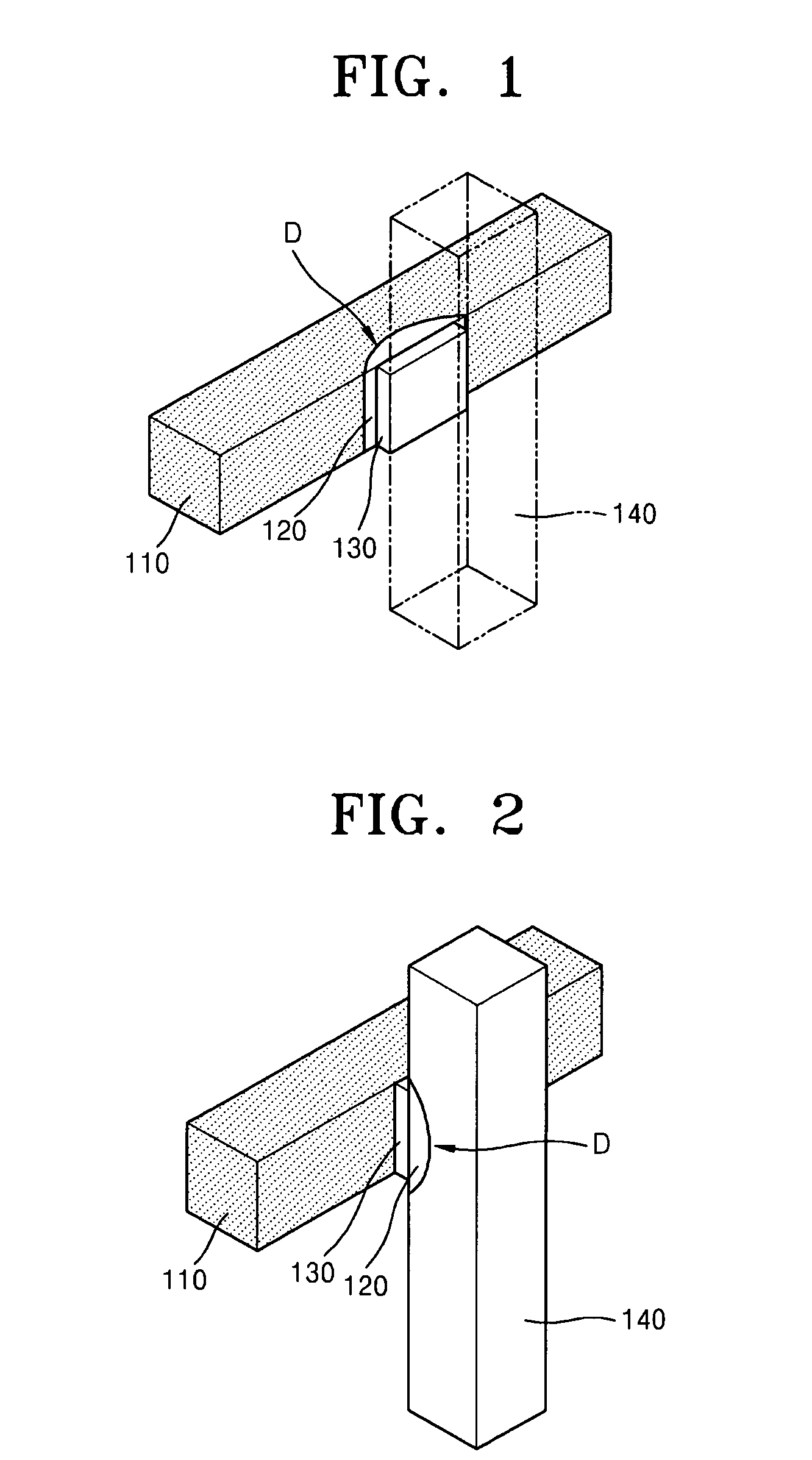
Figure 2 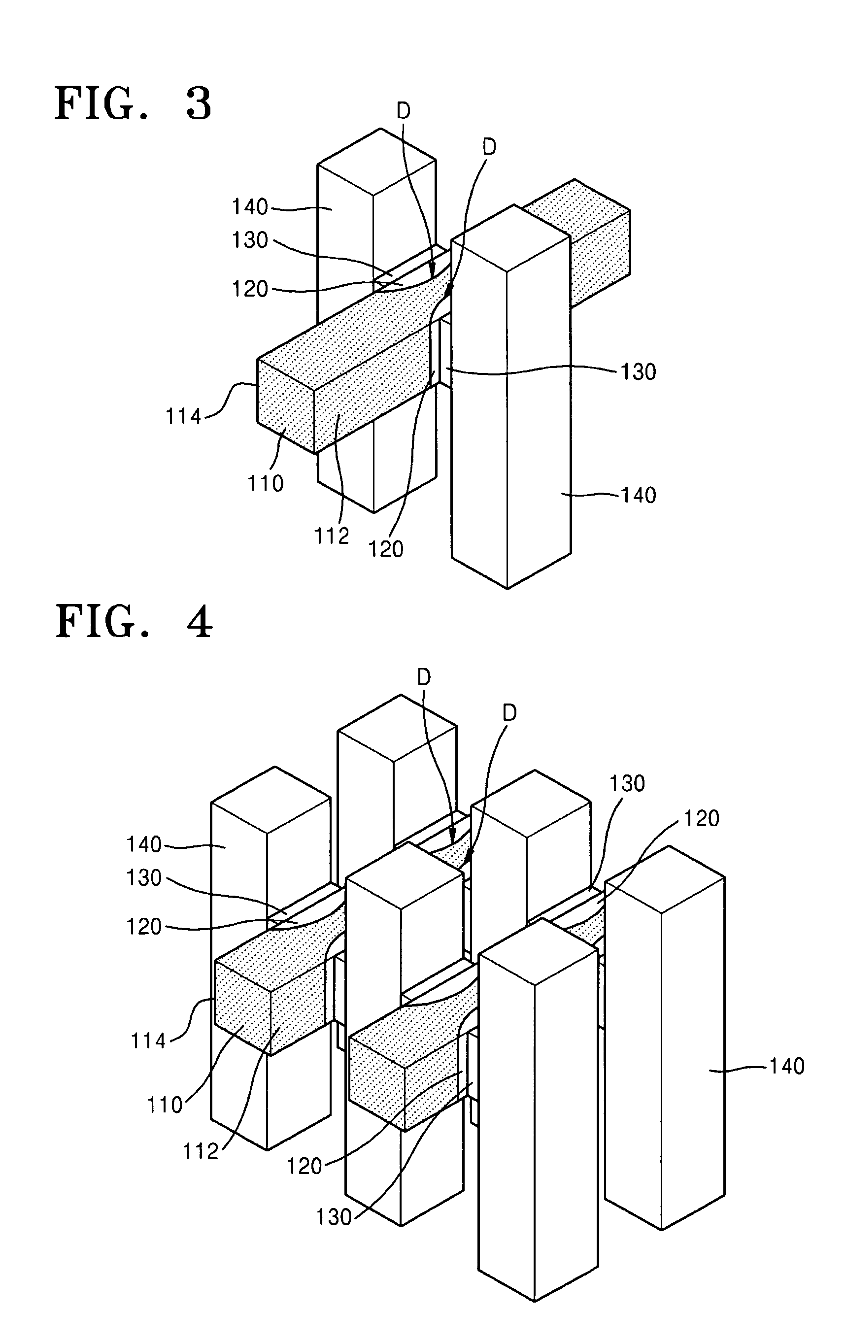
Figure 3
Abstract
Description
PRIORITY STATEMENT
[0001] This application claims priority under U.S.C. §119 to Korean Patent Application No. 10-2008-0035217, filed on Apr. 16, 2008, in the Korean Intellectual Property Office (KIPO), the entire contents of which are incorporated herein by reference.BACKGROUND
[0002] 1. Field
[0003] Example embodiments relate to a semiconductor device, and more particularly, to a non-volatile memory device having a multilayer structure and a method of fabricating the non-volatile memory device.
[0004] 2. Description of the Related Art
[0005] Demands for semiconductor products with smaller volume and higher data processing capacity have increased. To satisfy these demands, the operation speed and the integration degree of non-volatile memory devices used in semiconductor products has to be increased. In this respect, non-volatile memory devices with a multilayer structure, rather than a conventional monolayer structure, are advantageous for higher integration.
[0006] When a multilayer structure...
Examples
Embodiment Construction
[0025]Hereinafter, example embodiments will be described in detail by explaining example embodiments with reference to the attached drawings. Example embodiments may, however, be embodied in many different forms and should not be construed as being limited to the embodiments set forth herein; rather, these embodiments are provided so that this disclosure will be thorough and complete, and will fully convey the concept of example embodiments to those of ordinary skill in the art. In the drawings, the sizes of elements are exaggerated for clarity.
[0026]It will be understood that when an element is referred to as being “connected” or “coupled” to another element, it can be directly connected or coupled to the other element or intervening elements may be present. In contrast, when an element is referred to as being “directly connected” or “directly coupled” to another element, there are no intervening elements present. As used herein the term “and / or” includes any and all combinations o...