Analysis of Thin Film Deposition Uniformity Across Large Substrates
SEP 28, 20259 MIN READ
Generate Your Research Report Instantly with AI Agent
Patsnap Eureka helps you evaluate technical feasibility & market potential.
Thin Film Deposition Evolution and Uniformity Goals
Thin film deposition technology has evolved significantly over the past several decades, transitioning from rudimentary vacuum evaporation methods to sophisticated atomic-level precision techniques. The journey began in the 1950s with basic thermal evaporation processes, progressing through the development of sputtering technologies in the 1960s and 1970s, to the emergence of chemical vapor deposition (CVD) systems in the 1980s. The 1990s witnessed the refinement of plasma-enhanced CVD and the introduction of atomic layer deposition (ALD), marking a pivotal advancement in achieving atomic-scale control over film growth.
The evolution trajectory has consistently aimed toward greater precision, enhanced uniformity, and increased scalability to accommodate larger substrate dimensions. This progression has been driven primarily by the semiconductor industry's relentless pursuit of Moore's Law, alongside emerging demands from display technologies, photovoltaics, and optical coatings sectors. Each advancement has addressed specific limitations of preceding technologies, particularly regarding film uniformity across increasingly larger substrates.
Current technological goals in thin film deposition uniformity center on achieving sub-nanometer thickness variation across ultra-large substrates exceeding 2 meters in diagonal measurement. This represents a formidable challenge as substrate dimensions continue to expand while tolerance for non-uniformity simultaneously decreases. The industry now targets uniformity variations below ±1% for critical applications, with some advanced semiconductor processes demanding even tighter tolerances of ±0.5% or better.
Beyond mere thickness uniformity, contemporary objectives encompass compositional homogeneity, crystallographic consistency, and uniform stress distribution throughout deposited films. These parameters have become increasingly critical as device performance becomes more sensitive to nanoscale variations in material properties. The industry is also pursuing enhanced energy efficiency in deposition processes, reduced material waste, and minimized environmental impact—factors that were previously secondary considerations but now represent primary design constraints.
The technological roadmap for the next decade focuses on developing intelligent deposition systems incorporating real-time monitoring and feedback mechanisms. These systems aim to dynamically adjust process parameters during deposition to compensate for emerging non-uniformities. Machine learning algorithms are increasingly being integrated to predict and preemptively correct potential uniformity issues before they manifest, representing a paradigm shift from reactive to predictive process control methodologies.
Achieving these ambitious uniformity goals across large substrates will require interdisciplinary innovations spanning materials science, plasma physics, fluid dynamics, and computational modeling. Success in this domain will unlock new possibilities in flexible electronics, architectural-scale smart surfaces, and next-generation display technologies that demand unprecedented combinations of size and precision.
Large-Area Coating Market Demand Analysis
The global market for large-area thin film coatings has experienced significant growth over the past decade, driven primarily by expanding applications in electronics, renewable energy, and architectural glass industries. Current market valuations indicate the large-area coating sector reached approximately 12 billion USD in 2022, with projections suggesting a compound annual growth rate of 7.8% through 2028.
The semiconductor and display industries represent the largest demand segments, collectively accounting for over 40% of the total market share. This is primarily due to the increasing production of larger display panels for televisions, monitors, and mobile devices, where coating uniformity directly impacts product quality and yield rates. Consumer electronics manufacturers are consistently demanding larger substrate processing capabilities with higher uniformity specifications to reduce defect rates.
Photovoltaic applications have emerged as the fastest-growing segment, with demand increasing at nearly 15% annually. This surge is driven by global renewable energy initiatives and the continuous effort to improve solar cell efficiency through advanced thin film technologies. The trend toward larger solar panels to reduce installation costs per watt has created specific challenges for coating uniformity across increasingly expansive substrates.
Architectural glass coating represents another substantial market segment, particularly with the growing emphasis on energy-efficient buildings. Smart windows and low-emissivity glass coatings require precise uniformity across large surfaces to ensure consistent performance in thermal management and optical clarity. The construction industry's shift toward sustainable building materials has accelerated demand for high-performance coated glass products.
Regional analysis reveals Asia-Pacific dominates the market with approximately 45% share, led by manufacturing hubs in China, South Korea, and Taiwan. North America and Europe follow with 25% and 20% respectively, with particular strength in high-value specialty coatings and research-intensive applications.
Customer requirements are evolving toward stricter uniformity specifications, with many industries now demanding thickness variations below ±2% across substrates exceeding two square meters. This represents a significant technical challenge that directly impacts production costs and final product performance. Market research indicates that manufacturers capable of achieving superior uniformity metrics can command premium pricing of 15-30% above industry averages.
The economic implications of improved coating uniformity are substantial. Industry analyses suggest that enhancing uniformity by just 1% can reduce material waste by up to 8% and increase production yields by 5-12% depending on the application, representing significant cost savings in high-volume manufacturing environments.
Current Challenges in Large Substrate Uniformity
Despite significant advancements in thin film deposition technologies, achieving uniform deposition across large substrates remains one of the most persistent challenges in the industry. As substrate dimensions continue to increase to meet demands for larger displays, solar panels, and other applications, the complexity of maintaining uniformity scales exponentially. Current manufacturing processes struggle with edge effects, where film thickness and properties deviate significantly near substrate boundaries, creating yield and performance issues.
Temperature gradients present a formidable obstacle, particularly in thermal deposition methods. Even minor variations of a few degrees across a large substrate can result in substantial differences in deposition rates and film properties. Advanced thermal management systems have been implemented, but complete elimination of these gradients remains elusive, especially as substrate sizes exceed 2 meters in some applications.
Gas flow dynamics significantly impact uniformity in chemical vapor deposition (CVD) and plasma-enhanced processes. Computational fluid dynamics models reveal complex flow patterns that create non-uniform precursor distribution across large areas. While showerhead designs have evolved to improve distribution, they cannot fully compensate for inherent flow physics at industrial scales, particularly at higher process pressures.
Plasma uniformity challenges are equally critical in plasma-assisted deposition techniques. The difficulty in maintaining consistent plasma density and energy across large areas leads to variations in film properties. Edge-to-center differences in plasma characteristics often result in thickness variations exceeding acceptable tolerances for advanced applications like semiconductor devices and high-performance displays.
Equipment scaling presents both engineering and economic barriers. Traditional scaling approaches often fail to maintain process parameters consistently across larger dimensions. The cost of specialized equipment capable of handling larger substrates increases disproportionately with size, creating economic constraints for manufacturers.
Material utilization efficiency decreases dramatically with substrate size expansion. Current systems typically achieve only 15-30% material utilization for large area depositions, with the remainder wasted as overspray or chamber deposits. This inefficiency drives up production costs and creates environmental concerns regarding material waste and energy consumption.
Metrology and quality control face significant limitations when applied to large substrates. Real-time monitoring techniques struggle to provide comprehensive data across the entire substrate area, making process control increasingly difficult. Post-deposition characterization often reveals uniformity issues only after significant material and processing investments have been made.
Current Uniformity Control Methodologies
01 Optimization of deposition chamber design
The design of the deposition chamber significantly impacts thin film uniformity. Key design elements include gas flow distribution systems, chamber geometry, and substrate positioning mechanisms. Advanced chamber designs incorporate features like optimized gas inlet configurations, uniform gas distribution plates, and precisely controlled exhaust systems to ensure homogeneous precursor distribution across the substrate surface, resulting in improved film thickness uniformity.- Gas flow control for uniform deposition: Controlling gas flow dynamics in deposition chambers is critical for achieving uniform thin film deposition. This includes optimizing gas inlet configurations, flow rates, and distribution systems to ensure homogeneous precursor delivery across the substrate surface. Advanced gas flow control systems can compensate for edge effects and prevent thickness variations, particularly in large-area substrates or complex geometries.
- Substrate rotation and movement mechanisms: Implementing substrate rotation and movement systems significantly improves thin film uniformity by averaging out deposition variations. These mechanisms include rotating substrate holders, oscillating platforms, and multi-axis movement systems that ensure all areas of the substrate receive equal exposure to deposition sources. Dynamic substrate positioning is particularly effective in compensating for inherent non-uniformities in plasma distribution or vapor flux.
- Temperature control and thermal management: Precise temperature control across the substrate is essential for uniform thin film growth. Thermal management systems include advanced heaters with multiple zones, temperature sensors for real-time monitoring, and thermal shields to prevent temperature gradients. Maintaining consistent temperature profiles eliminates variations in reaction rates and adsorption/desorption processes that would otherwise lead to thickness and composition non-uniformities.
- Plasma optimization techniques: For plasma-enhanced deposition processes, optimizing plasma parameters is crucial for film uniformity. This includes controlling plasma density, power distribution, and electromagnetic field configurations. Advanced techniques such as pulsed plasma, dual-frequency plasma systems, and magnetic field confinement help achieve more homogeneous plasma distribution across large substrates, resulting in more uniform thin film properties.
- In-situ monitoring and feedback control systems: Real-time monitoring and feedback control systems enable dynamic adjustments during the deposition process to maintain uniformity. These systems utilize optical sensors, ellipsometry, or mass spectrometry to continuously measure film thickness and properties across the substrate. The collected data feeds into control algorithms that automatically adjust process parameters such as gas flow, temperature, or power distribution to compensate for detected non-uniformities.
02 Process parameter control and monitoring
Precise control of process parameters is essential for achieving uniform thin film deposition. Critical parameters include temperature distribution, pressure stability, precursor flow rates, and plasma characteristics. Real-time monitoring systems with feedback control mechanisms help maintain optimal conditions throughout the deposition process. Advanced process control algorithms can dynamically adjust parameters to compensate for variations, ensuring consistent film properties across the substrate.Expand Specific Solutions03 Substrate rotation and movement techniques
Implementing substrate rotation and movement mechanisms significantly improves thin film uniformity by averaging out local deposition rate variations. Techniques include continuous rotation, oscillatory movement, and planetary rotation systems. These methods ensure that all areas of the substrate receive equal exposure to deposition conditions, minimizing edge effects and radial non-uniformities that commonly occur in static deposition processes.Expand Specific Solutions04 Advanced precursor delivery systems
Sophisticated precursor delivery systems enhance thin film uniformity by ensuring consistent supply of deposition materials. These systems include advanced vaporizers, liquid delivery systems with precise flow control, and multi-zone injection mechanisms. Innovations in precursor chemistry and delivery methods, such as pulsed delivery techniques and sequential introduction of reactants, help achieve more uniform film growth across large substrate areas.Expand Specific Solutions05 In-situ monitoring and correction methods
Real-time monitoring and correction systems enable dynamic adjustment of deposition parameters to maintain film uniformity. These methods utilize sensors that measure film thickness, composition, and other properties during deposition. Advanced systems incorporate optical monitoring, plasma diagnostics, and machine learning algorithms to detect non-uniformities and automatically implement corrective actions, resulting in significantly improved film quality and consistency across large substrates.Expand Specific Solutions
Key Industry Players in Thin Film Deposition
The thin film deposition uniformity market is currently in a growth phase, with increasing demand for advanced semiconductor and display manufacturing technologies driving market expansion. The global market size is estimated to exceed $15 billion, fueled by applications in electronics, photovoltaics, and optical coatings. Leading players include Applied Materials, Tokyo Electron, and ULVAC, who have established strong technological capabilities in precision deposition systems. Emerging competitors like ACM Research and AMEC are gaining market share through innovative approaches to uniformity challenges. Academic institutions such as MIT and Cornell University contribute fundamental research, while companies like Samsung Display and LG Chem represent key end-users driving requirements for larger substrates and higher precision. The technology continues to mature with advances in process control, simulation tools, and in-situ monitoring capabilities.
Applied Materials, Inc.
Technical Solution: Applied Materials has developed comprehensive solutions for thin film deposition uniformity across large substrates through their Advanced Patterning and Packaging (APP) systems. Their flagship Endura® platform utilizes Physical Vapor Deposition (PVD) technology with rotational substrate holders and multiple magnetron sources positioned strategically to ensure uniform material distribution. The system incorporates real-time monitoring with advanced sensors that provide feedback for dynamic adjustments during deposition. Their proprietary E3™ (Equipment Engineering & Embedded) technology enables precise control of process parameters including temperature gradients, gas flow dynamics, and plasma distribution to achieve uniformity better than ±2% across 300mm wafers. Applied Materials has also pioneered multi-zone heating elements and gas distribution systems that compensate for edge effects in large substrates.
Strengths: Industry-leading process control systems with real-time monitoring capabilities; extensive experience with large substrate processing; comprehensive simulation tools for predicting deposition patterns. Weaknesses: Higher capital equipment costs compared to competitors; complex systems require specialized maintenance and operation expertise; some solutions are optimized for semiconductor applications and may require adaptation for other industries.
ULVAC INC
Technical Solution: ULVAC has developed specialized thin film deposition systems focusing on uniformity across large substrates through their ENTRONTM series. Their approach combines advanced sputtering technology with proprietary gas flow control systems that create uniform plasma distribution. ULVAC's systems feature multi-cathode arrangements with independent power control to each target, allowing for precise compensation of edge effects and center-to-edge thickness variations. Their ECO-SHOT™ technology implements pulsed DC power supplies that prevent arcing while maintaining stable deposition rates across the entire substrate surface. For large display and solar panel applications, ULVAC has engineered linear scanning mechanisms that move substrates beneath optimized deposition zones at controlled speeds, achieving uniformity better than ±3% across Gen 10.5 glass substrates (2940mm × 3370mm). Their systems also incorporate in-situ optical monitoring that provides real-time feedback on film thickness during deposition.
Strengths: Specialized expertise in large-area coating systems for display and solar industries; advanced multi-zone process control; extensive experience with diverse substrate materials including flexible substrates. Weaknesses: Systems often require significant floor space for large substrate handling; higher power consumption compared to some competitors; specialized components may lead to longer lead times for replacement parts.
Critical Patents in Large-Area Deposition Technology
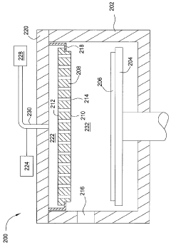
Gas distribution blocker apparatus
PatentWO2010065473A2
Innovation
- A gas distribution blocker apparatus is introduced, featuring a blocker member between the backing plate and showerhead, allowing for adjustable plenums and non-planar surface contours to alter the gas flow and pressure differential, ensuring uniform deposition across the substrate.
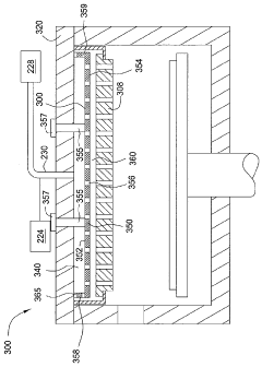
Deposition apparatus
PatentPendingUS20250137129A1
Innovation
- A deposition apparatus with a gas spraying part that varies in thickness along one direction, allowing for controlled gas flow and plasma density uniformity across the substrate, is designed. The gas spraying part has a curved surface in the non-vacuum state and a flat surface in the vacuum state to maintain consistent gap distances.
Material Science Considerations for Uniform Deposition
The material properties of both the substrate and the deposited film play a crucial role in achieving uniform thin film deposition across large substrates. Substrate characteristics such as thermal conductivity, surface roughness, and chemical composition directly impact the nucleation and growth mechanisms of thin films. Materials with higher thermal conductivity distribute heat more evenly during deposition processes, reducing temperature gradients that can cause thickness variations. Surface roughness at the microscopic level creates preferential nucleation sites, potentially leading to non-uniform growth patterns if not properly controlled.
Crystallographic orientation of the substrate material significantly influences epitaxial growth processes, where the atomic arrangement of the substrate guides the structural development of the deposited film. This becomes particularly important in applications requiring specific crystalline properties, such as semiconductor manufacturing and optoelectronic devices. The coefficient of thermal expansion (CTE) mismatch between substrate and film materials can induce stress during cooling, resulting in delamination, cracking, or warping that compromises uniformity.
The chemical compatibility between substrate and deposited material determines adhesion quality and interfacial reactions. Incompatible materials may form unwanted compounds at the interface or exhibit poor wetting characteristics, leading to island formation rather than continuous film growth. Surface energy considerations are equally important, as they govern how deposited atoms migrate across the substrate surface before incorporation into the growing film.
For large-area substrates, material homogeneity becomes increasingly challenging to maintain. Variations in dopant concentration, impurity levels, or structural defects across the substrate can create localized differences in deposition behavior. These variations often manifest as thickness non-uniformities or compositional gradients in the final film.
The choice of deposition material itself introduces additional complexity. Materials with high sticking coefficients tend to deposit where they first contact the substrate, potentially creating thickness variations near gas inlets in CVD processes or directly in line with sputtering targets. Conversely, materials with lower sticking coefficients allow for greater surface diffusion, which can enhance uniformity but may reduce deposition efficiency.
Alloying elements and dopants in the deposited material can segregate non-uniformly during growth, particularly if temperature gradients exist across the substrate. This phenomenon becomes more pronounced as substrate dimensions increase, requiring careful control of process parameters to maintain compositional uniformity throughout the film.
Equipment Scaling Factors for Industrial Applications
When scaling thin film deposition equipment for industrial applications, several critical factors must be considered to maintain uniformity across increasingly larger substrates. The transition from laboratory-scale to production-scale equipment introduces significant engineering challenges that directly impact film quality and process economics. Chamber geometry becomes a primary consideration, as the spatial relationship between deposition sources and substrates fundamentally changes with scale. Industrial systems typically require multiple deposition sources arranged in specific configurations to achieve acceptable uniformity across large areas, necessitating complex modeling of vapor flux distributions.
Source-to-substrate distance represents another crucial scaling parameter that must be optimized. While increasing this distance can improve uniformity through more diffuse vapor distribution, it simultaneously reduces deposition rates and material utilization efficiency. This trade-off becomes particularly significant in high-volume manufacturing environments where throughput considerations are paramount. Many industrial systems implement variable distance mechanisms that can be adjusted based on specific process requirements and substrate dimensions.
Thermal management systems must scale proportionally with substrate size to prevent temperature gradients that would otherwise lead to non-uniform film properties. Large substrates require sophisticated heating elements with multiple independently controlled zones, temperature sensors distributed across the substrate area, and enhanced thermal shielding to maintain consistent process conditions. The thermal mass of industrial-scale systems also necessitates longer stabilization times, which must be factored into process development and production scheduling.
Gas flow dynamics change dramatically with increased chamber volumes. Computational fluid dynamics modeling becomes essential for predicting gas distribution patterns and optimizing inlet/outlet configurations. Many industrial systems incorporate gas flow simulation capabilities directly into equipment design software to ensure uniform precursor delivery and byproduct removal across large substrate areas. Specialized gas distribution components, such as showerhead designs with hundreds or thousands of precisely engineered apertures, are often required.
Automation and control systems must scale in complexity to manage the increased number of process variables. Advanced process control strategies, including real-time monitoring and feedback mechanisms, become necessary to maintain uniformity specifications. Statistical process control methodologies are typically implemented to track key parameters across multiple deposition cycles, enabling predictive maintenance and process optimization. The integration of machine learning algorithms for pattern recognition in uniformity data represents the cutting edge of industrial equipment scaling.
Unlock deeper insights with Patsnap Eureka Quick Research — get a full tech report to explore trends and direct your research. Try now!
Generate Your Research Report Instantly with AI Agent
Supercharge your innovation with Patsnap Eureka AI Agent Platform!