How Thin Film Deposition Affects Optical Transparency in Devices
SEP 28, 20259 MIN READ
Generate Your Research Report Instantly with AI Agent
Patsnap Eureka helps you evaluate technical feasibility & market potential.
Thin Film Deposition Technology Evolution and Objectives
Thin film deposition technology has evolved significantly over the past century, transforming from rudimentary vacuum evaporation methods to sophisticated atomic-level precision techniques. The journey began in the early 20th century with thermal evaporation processes, which laid the foundation for modern thin film technologies. By the 1960s, sputtering techniques emerged, offering improved film uniformity and adhesion properties critical for optical applications.
The 1970s and 1980s witnessed the development of Chemical Vapor Deposition (CVD) methods, enabling the creation of films with superior optical transparency and controlled refractive indices. This period marked a pivotal shift from purely mechanical deposition to chemical reaction-based processes, significantly enhancing the optical quality of deposited films.
The advent of Atomic Layer Deposition (ALD) in the 1990s revolutionized the field by allowing atomic-level control over film thickness and composition. This precision became crucial for manufacturing high-performance optical devices with specific transparency requirements. Simultaneously, advances in Plasma-Enhanced CVD (PECVD) facilitated lower temperature deposition processes, expanding the range of substrate materials compatible with transparent film applications.
Recent technological breakthroughs include the development of High-Power Impulse Magnetron Sputtering (HiPIMS) and spatial ALD, which have dramatically increased deposition rates while maintaining excellent film quality. These innovations have addressed the historical trade-off between deposition speed and optical performance, enabling cost-effective production of high-transparency components.
The primary objective of thin film deposition technology in optical transparency applications is to achieve the optimal balance between light transmission, durability, and functionality. This involves developing films with precisely controlled thickness uniformity, minimal defect density, and tailored refractive indices. Additionally, the industry aims to enhance anti-reflective properties while maintaining excellent adhesion to various substrate materials.
Current research focuses on developing deposition techniques that can create multi-functional transparent films combining optical transparency with additional properties such as conductivity, hydrophobicity, or self-cleaning capabilities. The integration of these properties presents significant challenges but offers tremendous potential for next-generation display technologies, smart windows, and advanced optoelectronic devices.
Looking forward, the field is trending toward environmentally sustainable deposition methods that reduce energy consumption and eliminate hazardous precursors while maintaining optical performance. This evolution aligns with broader industry goals of developing greener manufacturing processes without compromising device functionality or optical transparency.
Market Demand for Optically Transparent Devices
The market for optically transparent devices has experienced significant growth over the past decade, driven primarily by the expanding consumer electronics sector. Smartphones, tablets, and wearable devices collectively represent the largest market segment requiring high-quality transparent components, with annual shipments exceeding 1.5 billion units globally. This demand has created a robust ecosystem for thin film deposition technologies that can deliver optimal optical transparency while maintaining other critical device properties.
Display technologies constitute the most substantial application area, with OLED and advanced LCD displays requiring increasingly sophisticated transparent conductive layers. The automotive industry has emerged as another significant market driver, with heads-up displays and smart windshields incorporating transparent thin films growing at a compound annual rate of approximately 22% since 2018. This growth trajectory is expected to continue as vehicle manufacturers integrate more advanced driver assistance systems requiring transparent interfaces.
Healthcare and medical devices represent a rapidly expanding market segment, with transparent biosensors and medical imaging equipment requiring specialized optical coatings. The global medical transparent film market reached $3.2 billion in 2022, with projections indicating continued strong growth through 2030. Thin film deposition techniques that can maintain biocompatibility while delivering optical clarity are particularly valued in this sector.
Smart building technologies incorporating transparent photovoltaics and electrochromic windows have created another substantial market opportunity. Commercial building retrofits focusing on energy efficiency have driven demand for these technologies, with the transparent conductive film market for architectural applications growing by 17% annually since 2020.
Consumer preferences have evolved to favor devices with seamless, transparent interfaces, creating pressure for manufacturers to develop increasingly sophisticated optical coatings. Market research indicates that consumers are willing to pay a premium of up to 15% for devices with superior display clarity and scratch resistance, directly influencing manufacturer investment in advanced thin film deposition technologies.
Regional market analysis reveals that East Asia dominates manufacturing capacity for optically transparent components, with China, South Korea, and Taiwan collectively accounting for over 65% of global production. However, recent supply chain disruptions have accelerated efforts to diversify manufacturing locations, with significant new investments in North America and Europe focused on specialized high-value transparent components requiring advanced deposition techniques.
Current Challenges in Transparent Thin Film Technology
Despite significant advancements in transparent thin film technology, several critical challenges continue to impede optimal performance in modern devices. The trade-off between transparency and conductivity remains one of the most persistent issues. As film thickness decreases to improve transparency, electrical conductivity often deteriorates, creating a fundamental engineering dilemma for applications requiring both properties, such as touchscreens and solar cells.
Material limitations present another significant hurdle. Traditional transparent conducting oxides (TCOs) like Indium Tin Oxide (ITO) face resource constraints due to indium scarcity, driving costs upward and necessitating alternative material development. However, alternative materials often struggle to match ITO's combination of high transparency and conductivity, particularly in the visible spectrum.
Deposition uniformity across large substrates poses substantial manufacturing challenges. As device dimensions increase, maintaining consistent film thickness and properties becomes exponentially more difficult. Edge effects, shadowing, and thermal gradients during deposition processes can lead to non-uniform film properties, affecting both optical and electrical performance across the substrate.
Interface and adhesion issues between thin films and substrates frequently lead to delamination and degradation over time. The thermal expansion coefficient mismatch between different materials creates stress during temperature fluctuations, compromising long-term device reliability. This is particularly problematic in flexible electronics applications where mechanical stress is inherent to operation.
Environmental stability presents ongoing concerns, as many transparent thin films degrade when exposed to moisture, oxygen, or UV radiation. This degradation manifests as decreased transparency, increased resistivity, or physical deterioration, significantly reducing device lifespan in real-world conditions.
Scalable manufacturing techniques that maintain film quality while enabling high-volume production remain elusive. While laboratory-scale deposition methods can produce excellent films, transitioning these processes to industrial scales often results in quality compromises or prohibitive costs. The balance between production speed, cost, and film quality continues to challenge manufacturers.
Emerging applications in flexible and stretchable electronics introduce additional requirements for mechanical durability while maintaining optical and electrical properties. Conventional brittle oxide films crack under strain, necessitating new materials and deposition approaches that can withstand repeated mechanical deformation without performance degradation.
The integration of multiple functional layers with minimal optical interference effects represents another frontier challenge, particularly for advanced devices requiring combinations of anti-reflection, touch-sensitivity, and display functionality within extremely limited thickness constraints.
Current Methods for Optimizing Optical Transparency
01 Deposition methods for optically transparent thin films
Various deposition techniques can be employed to create optically transparent thin films with controlled properties. These methods include chemical vapor deposition (CVD), physical vapor deposition (PVD), atomic layer deposition (ALD), and sputtering. Each technique offers different advantages in terms of film uniformity, thickness control, and optical transparency. The choice of deposition method significantly impacts the final optical properties of the thin film.- Transparent conductive oxide thin films: Transparent conductive oxide (TCO) films are deposited using various techniques to achieve high optical transparency while maintaining electrical conductivity. These films typically use materials such as indium tin oxide (ITO), zinc oxide, or aluminum-doped zinc oxide. The deposition parameters are optimized to achieve a balance between transparency in the visible spectrum and sufficient conductivity for electronic applications. These films are crucial for applications in displays, solar cells, and touch panels where both optical transparency and electrical functionality are required.
- Atomic layer deposition for optical films: Atomic layer deposition (ALD) techniques are employed to create highly uniform and conformal thin films with excellent optical transparency. This method allows precise control over film thickness at the atomic level, resulting in high-quality optical coatings with minimal defects. The layer-by-layer growth mechanism enables the creation of complex multilayer structures with tailored optical properties. ALD is particularly valuable for producing high-performance optical filters, anti-reflective coatings, and transparent barrier layers for sensitive devices.
- Sputtering methods for transparent films: Magnetron sputtering and other sputtering techniques are used to deposit optically transparent thin films with controlled composition and structure. These methods involve the ejection of material from a target source onto a substrate in a vacuum environment. Process parameters such as gas pressure, power, and substrate temperature are optimized to achieve films with high transparency and desired functional properties. Reactive sputtering, where the deposited material reacts with introduced gases, is particularly useful for creating oxide or nitride films with excellent optical characteristics.
- Chemical vapor deposition for transparent films: Chemical vapor deposition (CVD) techniques, including plasma-enhanced CVD, are utilized to create optically transparent thin films from gaseous precursors. These methods enable the deposition of high-quality dielectric films, semiconductors, and other materials with excellent optical transparency. The chemical reactions can be precisely controlled to achieve specific film compositions and structures that determine the optical properties. CVD processes are particularly valuable for large-area deposition of uniform transparent films for applications in optoelectronics, solar cells, and protective coatings.
- Post-deposition treatments for enhanced transparency: Various post-deposition treatments are applied to thin films to enhance their optical transparency and other properties. These include thermal annealing, laser treatment, plasma processing, and chemical treatments. Such processes can improve crystallinity, reduce defects, modify surface morphology, and optimize optical characteristics. Post-deposition treatments are essential for achieving the highest possible transparency while maintaining other functional properties such as conductivity or mechanical durability. These treatments can transform as-deposited films with moderate transparency into high-performance optical components.
02 Transparent conductive oxide (TCO) thin films
Transparent conductive oxide films combine high optical transparency with electrical conductivity, making them essential for optoelectronic applications. Materials such as indium tin oxide (ITO), zinc oxide (ZnO), and aluminum-doped zinc oxide (AZO) can be deposited as thin films with optimized transparency in the visible spectrum while maintaining good electrical properties. The composition, doping level, and deposition parameters significantly influence the balance between transparency and conductivity.Expand Specific Solutions03 Post-deposition treatments for enhanced transparency
Various post-deposition treatments can significantly improve the optical transparency of thin films. These include thermal annealing, plasma treatment, and surface modification techniques. Such treatments can reduce defects, improve crystallinity, and optimize the microstructure of the films, leading to enhanced optical properties. The temperature, duration, and atmosphere of these treatments are critical parameters that affect the final transparency of the thin films.Expand Specific Solutions04 Multi-layer thin film structures for optical applications
Multi-layer thin film structures can be designed to achieve specific optical properties such as anti-reflection, high reflection, or selective wavelength transmission. By carefully controlling the thickness and refractive index of each layer, these structures can enhance transparency in targeted wavelength ranges. The interface quality between layers and the overall stack design are crucial for achieving desired optical performance in applications such as optical filters, displays, and photovoltaic devices.Expand Specific Solutions05 Substrate preparation and interface control for transparent films
The preparation of substrates and control of interfaces are critical factors affecting the optical transparency of deposited thin films. Surface cleaning, planarization, and chemical modification of substrates can significantly improve film adhesion and reduce light scattering. Additionally, the introduction of buffer layers or interface engineering techniques can minimize defects and enhance the overall optical quality of the deposited films, resulting in improved transparency and performance.Expand Specific Solutions
Leading Companies in Thin Film Optical Technology
The thin film deposition technology for optical transparency in devices is currently in a growth phase, with the market expanding rapidly due to increasing demand for high-performance displays and optical components. The global market size is estimated to reach significant value as applications diversify across consumer electronics, automotive displays, and medical devices. Technologically, companies like Samsung Display, Corning, and BOE Technology are leading innovation with advanced deposition techniques that enhance transparency while maintaining functionality. OSRAM OLED, Semiconductor Energy Laboratory, and AUO Corp are developing specialized applications in OLED and TFT-LCD technologies. Meanwhile, research institutions like Industrial Technology Research Institute and Changchun Institute of Optics are pushing boundaries in next-generation transparent film technologies, creating a competitive landscape where material science expertise and manufacturing precision are key differentiators.
Semiconductor Energy Laboratory Co., Ltd.
Technical Solution: Semiconductor Energy Laboratory (SEL) has pioneered crystalline oxide semiconductor thin film technology that achieves both high electron mobility and optical transparency. Their CAAC-IGZO (C-Axis Aligned Crystalline Indium Gallium Zinc Oxide) deposition process creates highly ordered crystalline structures with transparency exceeding 80% across the visible spectrum while maintaining semiconductor properties[3]. SEL has developed specialized RF sputtering techniques that allow for precise control of oxygen content during deposition, which is critical for balancing transparency and conductivity in oxide films. Their multi-chamber deposition systems enable the creation of complex heterostructures with sharp interfaces between transparent layers with different functional properties. SEL's low-temperature deposition processes (below 400°C) enable the use of flexible plastic substrates while maintaining high transparency. Additionally, they've developed proprietary passivation layer technologies that protect transparent semiconductor films from environmental degradation while adding minimal optical absorption. Their recent innovations include self-aligned deposition techniques that reduce overlap capacitance in transparent thin film transistors while maintaining optical clarity across the device structure[7].
Strengths: World-leading expertise in oxide semiconductor physics; highly specialized deposition equipment optimized for transparent electronics; extensive patent portfolio covering key transparent semiconductor technologies. Weaknesses: Smaller manufacturing scale compared to major display manufacturers; some advanced materials require rare elements with supply constraints; specialized processes may have challenges scaling to very large substrate sizes.
Corning, Inc.
Technical Solution: Corning specializes in advanced glass technologies with their proprietary fusion draw process for thin film deposition, creating ultra-smooth, uniform glass substrates critical for optical transparency. Their Gorilla Glass technology incorporates ion-exchange strengthening while maintaining over 90% light transmission through precision-controlled deposition techniques. Corning's ClearCurve technology utilizes specialized coating methods that allow for flexible glass with minimal optical degradation when bent. Their vapor deposition processes create anti-reflective coatings that increase light transmission by reducing surface reflections from 4% to less than 0.5% per surface[1]. Additionally, Corning has developed specialized ITO (Indium Tin Oxide) sputtering techniques that achieve both high conductivity and transparency (>85% visible light transmission) for touchscreen applications, with thickness control at nanometer precision levels[3].
Strengths: Industry-leading expertise in glass substrate manufacturing with exceptional surface quality; proprietary fusion process creates atomically smooth surfaces ideal for display applications; advanced anti-reflective coatings significantly improve optical performance. Weaknesses: Higher cost compared to standard glass solutions; some specialized coatings require complex manufacturing processes that limit production scale; dependence on rare materials like indium for certain applications.
Key Patents in Transparent Thin Film Deposition
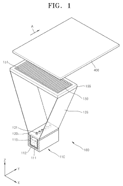
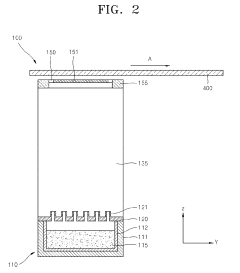
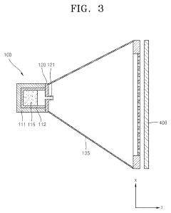
Thin film deposition apparatus
PatentInactiveUS20110088622A1
Innovation
- A thin film deposition apparatus with a patterning slit sheet that includes multiple sub-slits, allowing for overlapping patterns to form a desired shape, which is separate from the substrate by a predetermined distance, enabling continuous deposition while moving relative to each other, thus avoiding shadow zones and simplifying mask manufacturing.
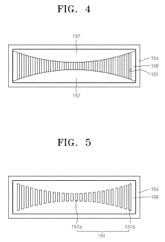
Thin film deposition apparatus
PatentPendingUS20190226078A1
Innovation
- A thin film deposition apparatus is designed with a deposition source, a deposition source nozzle unit, and a patterning slit sheet, where the substrate and apparatus move relative to each other, allowing continuous deposition and using a connection member to guide the material, with a correction plate to ensure uniform thickness and a tilted nozzle arrangement for improved uniformity.
Material Science Advancements for Optical Applications
Recent advancements in material science have revolutionized optical applications across multiple industries. The development of novel materials with enhanced optical properties has enabled significant improvements in device performance, particularly in displays, photovoltaics, and sensing technologies. These materials exhibit superior transparency, refractive index control, and spectral selectivity compared to conventional options.
Transparent conducting oxides (TCOs) represent one of the most significant breakthroughs, with indium tin oxide (ITO) and its alternatives such as aluminum-doped zinc oxide (AZO) and fluorine-doped tin oxide (FTO) offering exceptional combinations of electrical conductivity and optical transparency. These materials have become fundamental components in touchscreens, OLED displays, and thin-film solar cells.
Anti-reflective coatings have evolved from simple single-layer designs to sophisticated multi-layer structures that can reduce reflection across broad wavelength ranges. These coatings typically employ alternating high and low refractive index materials, with recent innovations incorporating nanostructured surfaces that mimic moth-eye patterns to achieve reflection values below 0.1% across the visible spectrum.
Metamaterials represent another frontier, engineered with sub-wavelength structures that enable unprecedented control over light propagation. These materials can exhibit negative refractive indices and other exotic optical properties not found in nature. Applications include super-resolution imaging systems, optical cloaking devices, and highly efficient light-harvesting structures.
Two-dimensional materials such as graphene and transition metal dichalcogenides (TMDs) have emerged as promising candidates for next-generation optical applications. Their atomically thin nature allows for exceptional light-matter interactions, while their tunable bandgaps enable precise control over optical absorption and emission properties. These materials show particular promise for ultrafast optical modulators and photodetectors.
Phase-change materials (PCMs) like germanium-antimony-tellurium (GST) compounds offer reversible switching between amorphous and crystalline states with dramatically different optical properties. This capability enables rewritable optical storage, programmable photonics, and tunable meta-surfaces that can dynamically control light propagation.
Perovskite materials have disrupted the photovoltaic landscape with their exceptional light absorption properties and solution processability. Beyond solar cells, these materials are finding applications in photodetectors, light-emitting diodes, and other optoelectronic devices where their tunable bandgap and high absorption coefficient provide significant advantages.
Environmental Impact of Thin Film Manufacturing Processes
The manufacturing processes involved in thin film deposition have significant environmental implications that warrant careful consideration. Traditional deposition methods such as physical vapor deposition (PVD) and chemical vapor deposition (CVD) often utilize hazardous precursor materials, including volatile organic compounds, heavy metals, and greenhouse gases. These substances can contribute to air pollution, water contamination, and soil degradation when improperly managed or released into the environment.
Energy consumption represents another critical environmental concern in thin film manufacturing. High-temperature processes like thermal evaporation and sputtering require substantial energy inputs, contributing to carbon emissions and resource depletion. For instance, maintaining vacuum conditions and plasma generation in magnetron sputtering systems demands continuous power supply, resulting in considerable energy footprints across production cycles.
Waste management challenges are particularly pronounced in optical thin film production. The pursuit of optimal transparency often involves multiple deposition-etching cycles, generating significant quantities of chemical waste. Etchants containing hydrofluoric acid, phosphoric acid, and other corrosive substances require specialized disposal protocols to prevent environmental contamination and protect ecosystem health.
Water usage represents another environmental dimension of thin film manufacturing. Cleaning processes between deposition stages typically consume large volumes of ultra-pure water, placing pressure on local water resources. The subsequent treatment of wastewater containing trace metals and chemical residues adds further complexity to the environmental management of these operations.
Recent technological innovations have begun addressing these environmental challenges. Atomic layer deposition (ALD) offers more precise material utilization, reducing waste generation compared to conventional methods. Additionally, the development of aqueous-based precursors and solvent-free deposition techniques has decreased reliance on environmentally harmful chemicals in certain applications.
Regulatory frameworks worldwide are increasingly focusing on the environmental aspects of thin film manufacturing. The European Union's Restriction of Hazardous Substances (RoHS) directive and similar regulations have prompted industry adaptation toward greener production methods. Life cycle assessment (LCA) approaches are now being applied to evaluate the comprehensive environmental impact of optical thin films from raw material extraction through manufacturing to end-of-life disposal.
The transition toward environmentally sustainable thin film production represents both a challenge and opportunity for the optoelectronics industry. Balancing the technical requirements for optical transparency with environmental responsibility will likely shape future research directions and manufacturing practices in this field.
Unlock deeper insights with Patsnap Eureka Quick Research — get a full tech report to explore trends and direct your research. Try now!
Generate Your Research Report Instantly with AI Agent
Supercharge your innovation with Patsnap Eureka AI Agent Platform!