Thin Film Deposition of Ferroelectric Materials for Nonvolatile Memory
SEP 28, 20259 MIN READ
Generate Your Research Report Instantly with AI Agent
Patsnap Eureka helps you evaluate technical feasibility & market potential.
Ferroelectric Thin Film Evolution and Research Objectives
Ferroelectric materials have undergone significant evolution since their discovery in the early 20th century. Initially identified in Rochelle salt in 1921, these materials gained prominence when barium titanate (BaTiO3) was discovered during World War II. The 1950s marked the beginning of systematic research into ferroelectric properties, with lead zirconate titanate (PZT) emerging as a dominant material due to its excellent ferroelectric characteristics and relatively simple processing requirements.
The 1980s witnessed a pivotal shift with the integration of ferroelectric materials into silicon-based microelectronics, particularly for nonvolatile memory applications. This period saw the development of various deposition techniques including sol-gel processing, sputtering, and chemical vapor deposition (CVD) methods, enabling the creation of high-quality thin films with controlled stoichiometry and crystallinity.
The 1990s brought significant advancements in perovskite-structured ferroelectrics such as PZT and strontium bismuth tantalate (SBT), which demonstrated promising characteristics for ferroelectric random access memory (FeRAM). Concurrently, researchers began exploring hafnium-based ferroelectrics, which would later revolutionize the field due to their CMOS compatibility.
Recent developments have focused on overcoming scaling limitations and improving reliability. The discovery of ferroelectricity in doped hafnium oxide (HfO2) in 2011 represented a breakthrough, offering CMOS compatibility, excellent scalability down to sub-10nm dimensions, and retention of ferroelectric properties at reduced thicknesses. This has opened new possibilities for ferroelectric field-effect transistors (FeFETs) and ferroelectric tunnel junctions (FTJs).
The current research landscape is characterized by efforts to optimize deposition techniques for these advanced materials. Atomic layer deposition (ALD) has emerged as a preferred method for creating ultra-thin, conformal ferroelectric films with precise thickness control and excellent uniformity, critical for next-generation memory devices.
Research objectives in this field now center on several key areas: enhancing the reliability and endurance of ferroelectric memories through improved material compositions and interface engineering; developing deposition processes that maintain ferroelectric properties at reduced dimensions; understanding and controlling polarization switching mechanisms at the nanoscale; and exploring novel device architectures that leverage ferroelectric properties for both memory and logic applications.
Additionally, researchers aim to address fundamental challenges related to wake-up effect, imprint, and fatigue phenomena that affect long-term device performance. The ultimate goal is to develop scalable, energy-efficient nonvolatile memory technologies that can meet the demands of future computing systems, including neuromorphic computing and in-memory processing architectures where ferroelectric materials show particular promise.
Market Analysis for Ferroelectric Nonvolatile Memory
The global market for ferroelectric nonvolatile memory is experiencing significant growth, driven by increasing demand for energy-efficient, high-speed, and reliable data storage solutions. Current market valuations place the ferroelectric memory sector at approximately 500 million USD in 2023, with projections indicating growth to reach 2.1 billion USD by 2028, representing a compound annual growth rate (CAGR) of 33.2%.
Key market drivers include the expanding Internet of Things (IoT) ecosystem, which requires low-power, persistent memory solutions for edge computing applications. The automotive industry represents another substantial growth vector, particularly with the transition toward electric and autonomous vehicles that demand robust memory systems capable of withstanding harsh operating conditions.
Consumer electronics continues to be the largest application segment, accounting for roughly 42% of the current market share. This dominance stems from the integration of ferroelectric memory in smartphones, wearables, and portable computing devices where power efficiency is paramount. Industrial automation and healthcare devices are emerging as rapidly growing segments, with expected CAGRs of 37% and 35% respectively over the next five years.
Regionally, Asia-Pacific dominates the market with approximately 58% share, primarily due to the concentration of semiconductor manufacturing facilities in countries like South Korea, Japan, and Taiwan. North America follows with 24% market share, driven by research initiatives and technology startups focused on advanced memory solutions. Europe accounts for 15% of the market, with particular strength in automotive and industrial applications.
Market challenges include competition from alternative memory technologies such as MRAM, ReRAM, and PCM, each offering distinct advantages in specific application scenarios. Cost factors remain significant, with current ferroelectric memory production costs approximately 30% higher than conventional DRAM on a per-bit basis, though this gap is narrowing as manufacturing processes mature.
Supply chain considerations are increasingly important, with raw material availability for certain ferroelectric compounds becoming a strategic concern. Hafnium-based materials, essential for advanced ferroelectric devices, have seen price volatility with increases of up to 45% in the past two years due to limited global supply sources.
Customer adoption patterns indicate growing acceptance in specialized high-reliability applications, with mainstream consumer adoption expected to accelerate once production costs decrease below the critical threshold of 1.5x compared to conventional memory technologies. This inflection point is anticipated within the next 24-36 months based on current technology development trajectories.
Current Challenges in Ferroelectric Thin Film Deposition
Despite significant advancements in ferroelectric thin film deposition techniques, several critical challenges persist that impede the widespread implementation of ferroelectric materials in nonvolatile memory applications. The primary challenge remains achieving consistent film quality with precise thickness control at the nanometer scale. As device dimensions continue to shrink following Moore's Law, the need for ultra-thin ferroelectric films (below 10 nm) becomes paramount, yet maintaining ferroelectric properties at such reduced dimensions is exceptionally difficult due to size effects that can suppress polarization.
Interface control presents another significant hurdle. The formation of dead layers at the electrode-ferroelectric interfaces can drastically reduce the effective polarization and increase the coercive field required for switching. These interfacial effects become increasingly dominant as film thickness decreases, creating a fundamental scaling limitation that must be overcome for next-generation memory devices.
Compositional control during deposition poses substantial difficulties, particularly for complex ferroelectric materials like PZT (lead zirconate titanate) or BFO (bismuth ferrite). Maintaining stoichiometry throughout the deposition process is challenging due to different volatilization rates of constituent elements, especially at elevated temperatures required for crystallization. Even minor deviations in composition can significantly alter electrical properties and reliability.
The crystallization temperature requirement presents another major obstacle. Most ferroelectric materials require high-temperature processing (>600°C) to achieve the desired crystalline phase, which conflicts with back-end-of-line (BEOL) integration requirements in semiconductor manufacturing, typically limited to 400°C. This thermal budget constraint severely restricts material choices and processing options.
Uniformity across large wafers remains problematic for industrial-scale production. Current deposition techniques struggle to maintain consistent thickness, composition, and crystallinity across 300mm wafers, resulting in device-to-device variability that is unacceptable for commercial memory applications.
Fatigue and retention characteristics also present significant challenges. Ferroelectric materials often exhibit polarization fatigue after repeated switching cycles and can suffer from retention loss over time. These reliability issues are exacerbated in thin films due to higher defect densities and greater susceptibility to environmental factors.
Compatibility with standard CMOS processing represents another critical challenge. Integration of ferroelectric materials often introduces contamination risks from elements like lead, bismuth, or zirconium that can degrade transistor performance. Developing effective diffusion barriers and contamination control strategies remains an ongoing challenge.
State-of-the-Art Deposition Techniques for Ferroelectric Films
01 Deposition techniques for high-quality ferroelectric thin films
Various deposition techniques can be employed to achieve high-quality ferroelectric thin films, including chemical vapor deposition (CVD), physical vapor deposition (PVD), pulsed laser deposition (PLD), and atomic layer deposition (ALD). Each technique offers specific advantages for controlling film thickness, composition, and crystallinity. The selection of an appropriate deposition method significantly impacts the final quality and properties of the ferroelectric thin film.- Deposition techniques for high-quality ferroelectric thin films: Various deposition techniques can be employed to create high-quality ferroelectric thin films, including chemical vapor deposition (CVD), physical vapor deposition (PVD), pulsed laser deposition (PLD), and atomic layer deposition (ALD). Each technique offers different advantages in terms of film uniformity, stoichiometry control, and crystallinity. The selection of an appropriate deposition method is crucial for achieving desired ferroelectric properties and film quality.
- Process parameters optimization for ferroelectric film quality: The quality of ferroelectric thin films is significantly influenced by process parameters such as substrate temperature, deposition pressure, gas flow rates, and annealing conditions. Optimizing these parameters is essential for controlling grain size, crystal orientation, and minimizing defects. Proper control of these variables leads to improved ferroelectric properties, including higher polarization, lower leakage current, and enhanced fatigue resistance.
- Substrate selection and preparation for ferroelectric thin films: The choice of substrate material and its preparation significantly impact the quality of deposited ferroelectric thin films. Substrates must have compatible crystal structures and thermal expansion coefficients with the ferroelectric material. Surface preparation techniques, including cleaning, etching, and buffer layer deposition, are crucial for achieving good adhesion, minimizing interfacial defects, and promoting epitaxial growth of the ferroelectric layer.
- Composition and doping strategies for enhanced ferroelectric properties: The composition of ferroelectric thin films can be modified through doping and alloying to enhance specific properties. Introducing dopants or creating complex oxide compositions can improve ferroelectric characteristics such as remnant polarization, coercive field, and Curie temperature. Careful control of stoichiometry and incorporation of specific elements can also reduce fatigue, imprint, and aging effects, leading to more reliable and higher-performing ferroelectric devices.
- Post-deposition treatments for ferroelectric film quality enhancement: Post-deposition treatments play a vital role in improving the quality of ferroelectric thin films. Thermal annealing in various atmospheres helps crystallize amorphous films, repair defects, and stabilize the ferroelectric phase. Other treatments like rapid thermal processing, oxygen annealing, and electric field cycling can further enhance ferroelectric properties by improving grain structure, reducing oxygen vacancies, and stabilizing domain configurations.
02 Process parameters optimization for ferroelectric film quality
Optimizing process parameters such as temperature, pressure, gas flow rates, and substrate conditions is crucial for achieving high-quality ferroelectric thin films. Precise control of these parameters affects crystallization, grain size, orientation, and ultimately the ferroelectric properties of the films. Post-deposition annealing treatments can also significantly improve film quality by enhancing crystallinity and reducing defects.Expand Specific Solutions03 Substrate selection and preparation for ferroelectric thin films
The choice and preparation of substrate materials significantly impact the quality of deposited ferroelectric thin films. Lattice matching between substrate and film, surface roughness, and crystallographic orientation of the substrate influence film growth, adhesion, and electrical properties. Buffer layers or seed layers can be used to improve compatibility between substrate and ferroelectric material, resulting in enhanced film quality and performance.Expand Specific Solutions04 Composition control and doping strategies for ferroelectric films
Controlling the composition and incorporating dopants in ferroelectric thin films can enhance their quality and functional properties. Precise stoichiometry control during deposition is essential for achieving optimal ferroelectric behavior. Doping with specific elements can modify electrical properties, improve crystallization, reduce leakage current, and enhance fatigue resistance of the films, leading to better overall performance in electronic devices.Expand Specific Solutions05 Characterization and quality assessment methods for ferroelectric thin films
Various analytical techniques are employed to assess the quality of ferroelectric thin films, including X-ray diffraction (XRD) for crystallinity and phase purity, scanning electron microscopy (SEM) for morphology, atomic force microscopy (AFM) for surface roughness, and electrical measurements for ferroelectric properties. These characterization methods help identify defects, impurities, and structural irregularities that may affect film performance, enabling process optimization for higher quality films.Expand Specific Solutions
Industry Leaders in Ferroelectric Memory Development
The ferroelectric thin film deposition market for nonvolatile memory is currently in a growth phase, with increasing demand driven by expanding applications in data storage. The global market is projected to reach significant scale as memory technologies evolve beyond traditional DRAM and NAND. Leading semiconductor manufacturers like Samsung Electronics, SK Hynix, and Intel are advancing the technology's maturity through substantial R&D investments. Academic institutions including Tsinghua University and Fudan University collaborate with industry players such as KIOXIA and Tokyo Electron to overcome technical challenges in material deposition uniformity and scalability. The competitive landscape features established memory producers competing with specialized equipment manufacturers, with Asian companies particularly dominant in commercialization efforts.
SK hynix, Inc.
Technical Solution: SK hynix has developed an advanced ferroelectric thin film deposition technology focused on hafnium-based materials for next-generation nonvolatile memory applications. Their approach employs a specialized atomic layer deposition (ALD) process that achieves precise thickness control down to 5nm while maintaining excellent ferroelectric properties[1]. SK hynix's technique incorporates aluminum doping of hafnium oxide to stabilize the ferroelectric orthorhombic phase at lower processing temperatures (350-450°C), making it compatible with back-end-of-line integration[2]. A distinctive aspect of their technology is the development of a "ferroelectric-dielectric" bilayer structure that optimizes both the ferroelectric switching properties and the leakage current characteristics, addressing a common challenge in scaled ferroelectric devices[3]. Their process demonstrates excellent uniformity across 300mm wafers with thickness variation below 2%, achieved through careful precursor delivery system design and chamber engineering. SK hynix has successfully integrated these films into both capacitor-based FeRAM and transistor-based FeFET structures, demonstrating data retention exceeding 10 years at 85°C and endurance of over 10^10 cycles in prototype devices[4].
Strengths: Excellent thickness uniformity across large wafers; innovative bilayer structure improving reliability; compatibility with both capacitor and transistor-based architectures. Weaknesses: Relatively complex process requiring precise doping control; potential challenges with scaling below 5nm; interface quality issues that may affect long-term reliability.
Samsung Electronics Co., Ltd.
Technical Solution: Samsung has pioneered advanced ferroelectric thin film deposition techniques for nonvolatile memory applications, particularly focusing on Hafnium Oxide (HfO2)-based ferroelectric random access memory (FRAM). Their approach utilizes atomic layer deposition (ALD) to create ultra-thin ferroelectric films with thicknesses below 10nm while maintaining excellent ferroelectric properties[1]. Samsung's process involves doping HfO2 with elements like silicon or zirconium to stabilize the ferroelectric orthorhombic phase, crucial for memory applications. They've developed a specialized annealing process that occurs at temperatures between 400-600°C to crystallize the ferroelectric phase without degrading the underlying CMOS structures[2]. Samsung has successfully integrated these ferroelectric films into 3D capacitor structures and has demonstrated working prototypes with endurance exceeding 10^12 cycles and data retention capabilities of over 10 years at 85°C[3], positioning their technology as a strong candidate for next-generation embedded nonvolatile memory applications.
Strengths: Industry-leading integration capabilities allowing ferroelectric materials to be incorporated into existing CMOS processes; exceptional endurance and retention characteristics; scalability to sub-10nm nodes. Weaknesses: Higher processing temperatures compared to some competing technologies; challenges with uniform deposition over high-aspect-ratio 3D structures; potential wake-up and fatigue effects requiring additional engineering solutions.
Critical Patents and Research in Ferroelectric Material Engineering
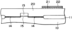
Manufacturing method for ferroelectric film and nonvolatile memory using the same
PatentInactiveUS6114199A
Innovation
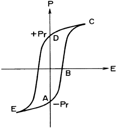
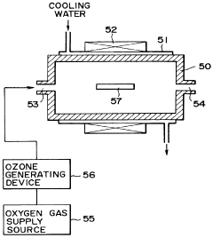
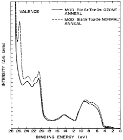
- A forming method involving heat treatment in an active oxygen atmosphere, using oxidizing gases like ozone, N2O, or NO2, to securely oxidize metal atoms and reduce oxygen defects, with specific conditions for temperature, concentration, and time to enhance oxygen diffusion and crystallinity.
Rare earth manganate films made by metalorganic decomposition or metalorganic chemical vapor deposition for nonvolatile memory devices
PatentInactiveUS5625587A
Innovation
- The use of rare earth manganate films with a perovskite structure, applied using metalorganic chemical vapor deposition (MOCVD) or metalorganic decomposition (MOD) methods, offers high Curie temperature, saturation polarization, and small dielectric constant, reducing defect migration and entrapment, and eliminating the need for high temperature annealing.
Material Compatibility and Integration Considerations
The integration of ferroelectric materials into semiconductor manufacturing processes presents significant challenges that must be addressed for successful commercialization of ferroelectric nonvolatile memory devices. Material compatibility issues arise primarily at the interfaces between the ferroelectric layer and adjacent materials, including electrodes, barrier layers, and the silicon substrate.
Electrode material selection is critical as it directly impacts the ferroelectric properties and device performance. Platinum and ruthenium are commonly used due to their chemical stability and work function compatibility, but they present integration challenges with standard CMOS processes. Noble metals may require additional adhesion layers, complicating the fabrication sequence and potentially introducing unwanted interfacial reactions.
Thermal budget constraints represent another major consideration. Many ferroelectric materials, particularly perovskites like PZT and BTO, require high-temperature processing (>600°C) for crystallization and optimal ferroelectric properties. However, these temperatures can cause interdiffusion, reaction with silicon, and degradation of underlying CMOS structures. Lower temperature deposition techniques such as atomic layer deposition with enhanced crystallization methods are being developed to address this limitation.
Diffusion barriers are essential to prevent elemental migration between layers. Without proper barriers, oxygen, lead, or other elements from ferroelectric materials can diffuse into silicon, forming undesirable interfacial layers that degrade device performance. TiN, TaN, and SrRuO3 have shown promise as effective barrier materials, but their integration requires precise thickness control and deposition conditions.
Stress management is another critical factor affecting material compatibility. The mismatch in thermal expansion coefficients between ferroelectric films and substrates can induce mechanical stress during thermal cycling, potentially leading to film cracking, delamination, or altered ferroelectric properties. Buffer layers and stress-relief structures are often incorporated to mitigate these effects.
Scaling considerations further complicate integration efforts. As device dimensions shrink below 100 nm, maintaining ferroelectric properties becomes increasingly challenging due to size effects. The critical thickness for ferroelectricity varies by material, with HfO2-based systems showing advantages for ultra-thin applications compared to traditional perovskites.
Contamination control represents a significant integration challenge, as many ferroelectric materials contain elements (like Pb, Zr, Ba) that are considered contaminants in standard CMOS facilities. Dedicated equipment or strict process isolation protocols are typically required to prevent cross-contamination, adding complexity and cost to manufacturing processes.
Scaling Challenges for Commercial Ferroelectric Memory Production
The commercialization of ferroelectric memory technologies faces significant scaling challenges that must be addressed before widespread adoption can occur. As device dimensions continue to shrink below 40nm, maintaining the ferroelectric properties becomes increasingly difficult. The crystalline structure of ferroelectric materials like PZT and BTO exhibits degraded polarization characteristics at reduced thicknesses, with a critical threshold around 5-10nm where ferroelectricity may disappear entirely.
Manufacturing consistency presents another major hurdle. Current thin film deposition techniques struggle to achieve uniform ferroelectric layers across large wafers, resulting in performance variations that are unacceptable for high-volume memory production. The industry standard 300mm wafer processes show edge-to-center thickness variations exceeding 5%, significantly impacting device yield and reliability.
Integration with CMOS processes introduces thermal budget constraints that limit material choices and processing options. Most ferroelectric materials require high-temperature annealing (>600°C) to achieve proper crystallization, which can damage underlying CMOS structures and metallization layers. This creates a fundamental conflict between optimizing ferroelectric properties and maintaining compatibility with standard semiconductor manufacturing flows.
Electrode interface engineering represents another critical scaling challenge. As devices shrink, the interface between the ferroelectric material and electrodes becomes increasingly dominant in determining overall device performance. Oxygen vacancies, interdiffusion, and work function mismatches at these interfaces can significantly degrade polarization retention and endurance characteristics, particularly at elevated operating temperatures.
The etching processes for ferroelectric materials present unique difficulties compared to conventional semiconductor materials. Achieving high-aspect-ratio structures with clean sidewalls becomes extremely challenging below 100nm feature sizes. Current plasma etching techniques often introduce surface damage that degrades ferroelectric properties at the pattern edges, reducing effective device performance.
Long-term reliability testing reveals additional concerns for scaled ferroelectric devices. Fatigue mechanisms, imprint effects, and retention loss accelerate at smaller dimensions due to increased influence of defects and domain wall dynamics. Commercial memory applications typically require 10-year data retention and 10^15 write cycle endurance—metrics that become increasingly difficult to achieve as dimensions shrink below 28nm nodes.
Unlock deeper insights with Patsnap Eureka Quick Research — get a full tech report to explore trends and direct your research. Try now!
Generate Your Research Report Instantly with AI Agent
Supercharge your innovation with Patsnap Eureka AI Agent Platform!