Standards and Qualification Procedures for Thin Film Deposition Processes
SEP 28, 202510 MIN READ
Generate Your Research Report Instantly with AI Agent
Patsnap Eureka helps you evaluate technical feasibility & market potential.
Thin Film Deposition Technology Evolution and Objectives
Thin film deposition technology has evolved significantly over the past century, transitioning from rudimentary vacuum evaporation methods to sophisticated atomic-level precision techniques. The journey began in the early 20th century with thermal evaporation processes, which laid the foundation for modern thin film applications. By the 1960s, sputtering technologies emerged as viable alternatives, offering improved film uniformity and adhesion properties for industrial applications.
The 1970s marked a pivotal shift with the introduction of Chemical Vapor Deposition (CVD) techniques, enabling the creation of films with complex compositions and structures. This period also witnessed the development of Plasma-Enhanced CVD (PECVD), which allowed for lower temperature deposition processes critical for temperature-sensitive substrates. The subsequent decades saw rapid advancement in precision and control, culminating in Atomic Layer Deposition (ALD) in the 1990s, which revolutionized the semiconductor industry by enabling atomic-level thickness control.
Recent technological evolution has focused on enhancing process efficiency, reducing environmental impact, and expanding application versatility. Innovations such as High-Power Impulse Magnetron Sputtering (HiPIMS) and Spatial ALD have addressed throughput limitations while maintaining film quality. Additionally, the integration of in-situ monitoring systems has significantly improved process control and reproducibility, addressing key standardization challenges.
The primary objectives in thin film deposition standardization encompass establishing universal metrics for film quality assessment, developing comprehensive qualification procedures, and creating industry-wide certification protocols. These standards aim to ensure consistency across different deposition technologies and equipment manufacturers, facilitating quality assurance in critical applications such as semiconductor fabrication, optical coatings, and medical devices.
A key goal is the development of standardized testing methodologies that can reliably evaluate film properties including thickness uniformity, adhesion strength, compositional purity, and structural integrity. These methodologies must be applicable across various substrate materials and geometries to accommodate the diverse range of industrial applications.
Looking forward, the technology trajectory points toward increased automation and integration with artificial intelligence for process optimization. The industry is moving toward "smart" deposition systems capable of self-calibration and adaptive processing based on real-time feedback. This evolution necessitates new standardization approaches that can accommodate these advanced capabilities while ensuring backward compatibility with established qualification procedures.
The ultimate objective remains the establishment of globally recognized standards that balance technological innovation with practical implementation requirements, enabling consistent quality assessment across geographical and technological boundaries in thin film deposition processes.
Industrial Applications and Market Demand Analysis
Thin film deposition processes have become integral to numerous high-value industrial sectors, driving significant market demand across diverse applications. The semiconductor industry represents the largest market segment, with thin film technologies being essential for manufacturing integrated circuits, memory devices, and microprocessors. According to market research, the semiconductor thin film equipment market exceeded $20 billion in 2022, with a projected compound annual growth rate of 6.8% through 2028, primarily driven by the increasing complexity of chip architectures and the transition to smaller node sizes.
The display technology sector constitutes another substantial market, with thin film deposition being critical for manufacturing LCD, OLED, and emerging microLED displays. The precision coating capabilities enable the production of high-resolution, energy-efficient displays for consumer electronics, automotive interfaces, and professional applications. This segment is experiencing rapid growth due to increasing consumer demand for higher display quality and the expansion of display technology into new product categories.
In the renewable energy sector, thin film solar cells represent a growing application area, with technologies such as CIGS (copper indium gallium selenide) and CdTe (cadmium telluride) offering advantages in flexibility, weight reduction, and performance under diffuse light conditions. The global thin film solar cell market is expanding at approximately 12% annually, reflecting the increasing focus on sustainable energy solutions and the improving cost-effectiveness of thin film photovoltaic technologies.
The optical coating industry utilizes thin film deposition for producing anti-reflective coatings, optical filters, and specialized mirrors for applications ranging from eyewear to precision scientific instruments. This market segment values highly standardized deposition processes that ensure consistent optical performance across production batches.
Medical device manufacturing represents an emerging high-value application area, with thin film coatings being used to enhance biocompatibility, create antimicrobial surfaces, and improve the performance of implantable devices. The stringent regulatory environment in this sector creates particularly strong demand for well-documented, validated deposition processes with comprehensive qualification procedures.
Aerospace and defense applications require specialized thin film coatings for thermal management, wear resistance, and sensor technologies. These applications typically demand the highest levels of process qualification and material performance verification, creating a premium market segment for advanced deposition technologies with robust quality assurance protocols.
The automotive industry increasingly utilizes thin film technologies for functional coatings on components, sensors, and display systems. With the transition to electric vehicles and advanced driver assistance systems, the demand for specialized thin film components is growing substantially, creating new market opportunities for qualified deposition processes.
Global Standards Landscape and Technical Challenges
The global landscape for thin film deposition standards presents a complex and fragmented picture, with significant variations across regions and industries. Major standards organizations such as ISO, ASTM International, SEMI, and IEC have established various specifications, but there remains a lack of comprehensive harmonization. This fragmentation creates challenges for manufacturers operating in global markets, as they must navigate multiple certification requirements across different jurisdictions.
In North America, ASTM standards predominate, with ASTM E3175 and F1711 specifically addressing thin film measurement and characterization. Meanwhile, the European landscape is shaped by ISO standards and regional specifications like DIN in Germany. Asian markets, particularly Japan and South Korea, have developed their own robust standards frameworks through organizations like JEITA and KATS, often with unique requirements that reflect their manufacturing priorities.
Technical challenges in standardization are multifaceted. The increasing complexity of multilayer thin film structures used in advanced electronics and photovoltaics demands more sophisticated measurement protocols than current standards provide. Many existing standards were developed for traditional applications and struggle to address novel materials like 2D materials, high-entropy alloys, and complex oxides used in emerging technologies.
Metrology presents another significant challenge, as measurement techniques vary in resolution, accuracy, and applicability across different film thicknesses and material compositions. This creates difficulties in establishing universally applicable qualification procedures. The industry faces a particular gap in standardized in-situ monitoring techniques, which are becoming increasingly important for real-time process control in high-precision applications.
Environmental considerations are driving new standardization needs, with growing emphasis on reducing hazardous materials and improving energy efficiency in deposition processes. However, standards development in this area remains nascent, creating regulatory uncertainty for manufacturers.
The rapid pace of technological innovation further complicates standardization efforts. New deposition techniques like atomic layer deposition (ALD) and spatial ALD are advancing faster than standards bodies can respond, creating a standards lag that impacts quality assurance frameworks. This is particularly problematic in emerging applications like flexible electronics, quantum computing components, and biomedical coatings, where established qualification procedures may not adequately address novel performance requirements.
Cross-industry collaboration remains insufficient, with standards often developed in silos despite thin film technologies spanning multiple sectors from semiconductors to medical devices. This fragmentation impedes knowledge transfer and creates redundancies in standards development efforts.
Current Qualification Methodologies and Protocols
01 Standardization of thin film deposition processes
Standardization is crucial for ensuring consistency and quality in thin film deposition processes. This involves establishing specific parameters, protocols, and metrics that define acceptable quality levels. These standards help in maintaining uniformity across different manufacturing batches and equipment, enabling reliable production of thin films with consistent properties. Standardization also facilitates comparison between different deposition techniques and ensures compliance with industry requirements.- Standardization of thin film deposition equipment and processes: Standards for thin film deposition equipment and processes ensure consistent quality and performance. These standards cover equipment specifications, process parameters, and operational procedures. Standardization helps in maintaining uniformity across different manufacturing facilities and enables reliable production of thin films with desired properties. Qualification procedures for deposition equipment include verification of chamber conditions, gas flow rates, and temperature control systems.
- Quality control and testing methods for thin film deposition: Quality control methods for thin film deposition involve various testing procedures to verify film properties. These include thickness measurement, uniformity assessment, adhesion testing, and compositional analysis. Advanced analytical techniques such as ellipsometry, X-ray diffraction, and electron microscopy are employed to characterize deposited films. In-situ monitoring systems provide real-time feedback during the deposition process, allowing for immediate adjustments to maintain quality standards.
- Qualification procedures for semiconductor manufacturing: Qualification procedures specific to semiconductor manufacturing involve rigorous testing of thin film properties relevant to device performance. These procedures include electrical characterization, stress testing, and reliability assessment of deposited films. Process qualification involves statistical analysis of multiple deposition runs to ensure repeatability and consistency. Equipment qualification procedures verify that deposition tools meet specifications for semiconductor-grade thin films, including contamination control and precision requirements.
- Calibration and maintenance protocols for deposition systems: Calibration and maintenance protocols are essential for ensuring the long-term reliability of thin film deposition systems. Regular calibration of critical parameters such as gas flow controllers, pressure sensors, and temperature monitors maintains process accuracy. Preventive maintenance schedules include chamber cleaning, target replacement, and vacuum system inspection. Documentation of calibration and maintenance activities is required for compliance with quality standards and for troubleshooting process deviations.
- International standards and certification for thin film processes: International standards organizations provide frameworks for thin film deposition processes across various industries. These standards include specifications for process validation, equipment qualification, and quality management systems. Certification requirements may vary by application, with more stringent standards for critical applications in aerospace, medical devices, and advanced electronics. Compliance with international standards facilitates global manufacturing and ensures product acceptance in international markets.
02 Qualification procedures for deposition equipment
Qualification procedures for thin film deposition equipment involve systematic testing and validation to ensure that the equipment meets specified performance criteria. These procedures typically include installation qualification (IQ), operational qualification (OQ), and performance qualification (PQ). Equipment qualification may involve calibration, verification of critical parameters, and demonstration of process capability. Regular qualification helps in maintaining the reliability and consistency of the deposition processes.Expand Specific Solutions03 In-situ monitoring and quality control methods
In-situ monitoring techniques are employed during thin film deposition to ensure real-time quality control. These methods include optical monitoring, plasma diagnostics, and sensor-based feedback systems that allow for immediate adjustments to process parameters. Real-time monitoring helps in detecting deviations from standard conditions, reducing defects, and ensuring film uniformity. Advanced monitoring systems can integrate with automated control systems to maintain process stability and optimize film properties.Expand Specific Solutions04 Process validation and certification protocols
Validation and certification protocols for thin film deposition processes involve comprehensive testing and documentation to demonstrate that the process consistently produces films meeting predetermined specifications. These protocols typically include process characterization, identification of critical parameters, establishment of acceptable ranges, and statistical analysis of results. Certification may require third-party verification and compliance with international standards. Validated processes ensure reproducibility and reliability in thin film manufacturing.Expand Specific Solutions05 Advanced metrology techniques for film qualification
Advanced metrology techniques are essential for qualifying thin films against established standards. These techniques include ellipsometry, X-ray reflectivity, atomic force microscopy, and spectroscopic methods that provide detailed information about film thickness, composition, structure, and properties. Metrology data is used to verify compliance with specifications and to identify process variations. Automated metrology systems enable high-throughput qualification of films in production environments, ensuring consistent quality across large substrate areas.Expand Specific Solutions
Leading Organizations and Industry Stakeholders
The thin film deposition process standards and qualification landscape is evolving rapidly in a maturing market estimated at $15-20 billion annually. The industry is transitioning from early growth to standardization phase, with major semiconductor and display manufacturers driving requirements. Key players include established equipment providers like Tokyo Electron, Samsung Electronics, and ASM IP Holding alongside emerging specialists such as WONIK IPS, NAURA Microelectronics, and Jiangsu Leadmicro. Technical maturity varies significantly across deposition methods, with ALD and PECVD technologies reaching higher standardization levels than emerging techniques. Research institutions like Nanjing University and KU Leuven collaborate with industry leaders to develop next-generation qualification procedures, particularly for advanced applications in semiconductor and display manufacturing.
Beijing NAURA Microelectronics Equipment Co., Ltd.
Technical Solution: NAURA has established a comprehensive qualification system for thin film deposition processes that combines international standards with specialized protocols for semiconductor manufacturing. Their qualification framework implements a multi-stage approach beginning with equipment qualification that verifies hardware performance against design specifications, followed by process qualification that validates film properties against application requirements. NAURA's standards include detailed protocols for characterizing film thickness uniformity (targeting <±2% variation across 300mm wafers), composition uniformity (verified through XPS/AES analysis at multiple points), and defect density (typically <0.1 defects/cm² for particles >0.3μm). Their qualification procedures incorporate extensive process capability studies using statistical methods to determine optimal process windows and identify critical parameters affecting film quality. NAURA has developed specialized test structures for evaluating electrical and mechanical properties of deposited films, with standardized measurement protocols for resistivity, stress, adhesion strength, and other application-specific parameters. Their qualification system also includes accelerated reliability testing under various environmental conditions to predict long-term stability of the deposited films.
Strengths: Strong integration of international standards with specialized protocols for semiconductor applications enables broad compatibility while addressing industry-specific requirements. Their comprehensive statistical approach to process capability studies ensures robust manufacturing processes. Weaknesses: Their qualification framework is primarily optimized for semiconductor applications and may require adaptation for other industries. The extensive characterization requirements necessitate significant investment in advanced analytical equipment and expertise.
Samsung Electronics Co., Ltd.
Technical Solution: Samsung Electronics has developed an integrated qualification framework for thin film deposition processes that spans their semiconductor, display, and advanced materials divisions. Their approach incorporates a standardized "Process Capability Index" (Cpk) methodology requiring all qualified processes to maintain a Cpk >1.67, ensuring six-sigma quality levels. Samsung's qualification procedures include comprehensive physical characterization requirements with standardized sampling plans across production lots. Their thin film standards specify not only thickness uniformity (typically <±2% for 300mm wafers) but also detailed requirements for film stress (measured via wafer bow techniques), crystallinity (via XRD analysis), and interface quality (via high-resolution TEM). Samsung has implemented automated Statistical Process Control (SPC) systems that continuously monitor critical parameters during deposition, with standardized response protocols when parameters drift beyond established control limits. Their qualification procedures include accelerated environmental testing under conditions exceeding application requirements, with standardized test structures for evaluating reliability factors including adhesion strength, thermal stability, and resistance to environmental contaminants.
Strengths: Comprehensive integration across multiple technology platforms enables knowledge transfer between different applications. Their statistical approach with strict Cpk requirements ensures exceptional consistency in high-volume manufacturing. Weaknesses: The qualification framework is highly optimized for their internal manufacturing ecosystem and may be challenging to implement in different operational environments. The extensive characterization requirements demand significant investment in advanced analytical equipment.
Key Standards and Certification Documentation
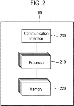
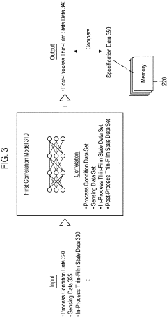
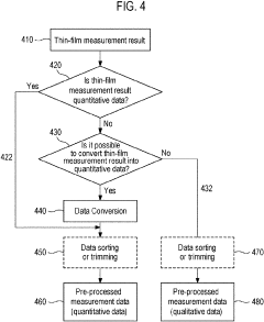
Apparatus, method, and recording medium storing command for controlling thin-film deposition process
PatentActiveUS20230279538A1
Innovation
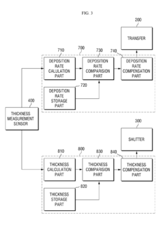
- A machine learning-based apparatus that communicates with thin-film deposition devices, sensors, and measurement tools to derive post-process thin-film state data using correlation models established from process condition, sensing, and in-process data, enabling comprehensive analysis and improving reliability by converting qualitative data into quantitative form and adjusting process conditions accordingly.
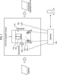
Thin film deposition apparatus and method
PatentInactiveUS20160186313A1
Innovation
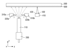
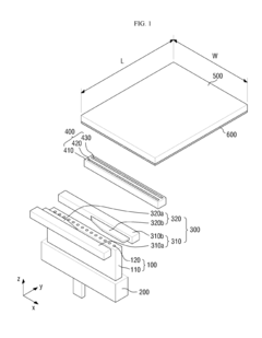
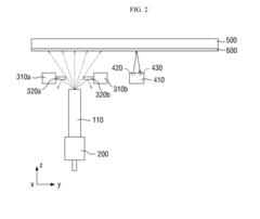
- A deposition apparatus equipped with a deposition source, a transfer unit, a thickness measurement sensor, and a transfer controller that adjusts the moving speed of the transfer unit based on real-time thickness measurements, and a shutter system that controls the emission region of the deposition material to maintain uniform film thickness.
Quality Control and Testing Frameworks
Quality control and testing frameworks for thin film deposition processes have evolved significantly over the past decade, establishing comprehensive methodologies to ensure consistent film quality across various applications. These frameworks typically incorporate multiple testing regimes operating at different stages of the production process, from pre-deposition material verification to post-deposition performance evaluation.
The cornerstone of modern quality control systems for thin films is in-situ monitoring, which allows real-time assessment of film growth parameters. Techniques such as spectroscopic ellipsometry, quartz crystal microbalance (QCM), and optical emission spectroscopy provide continuous feedback on deposition rates, thickness uniformity, and composition. These methods have demonstrated capability to detect deviations as small as 1-2 nanometers in film thickness, enabling immediate process adjustments before defects propagate.
Post-deposition characterization forms another critical component of testing frameworks, typically involving a combination of physical, chemical, and electrical measurements. Surface profilometry, atomic force microscopy (AFM), and scanning electron microscopy (SEM) are routinely employed to evaluate topographical features and structural integrity. X-ray diffraction (XRD) and X-ray photoelectron spectroscopy (XPS) provide insights into crystallinity and chemical composition, respectively.
Statistical process control (SPC) methodologies have been increasingly integrated into thin film quality frameworks, with control charts and capability indices becoming standard tools for monitoring process stability. Advanced manufacturers now implement automated systems that track critical parameters across multiple deposition runs, establishing baseline performance metrics and identifying subtle drift patterns before they result in specification violations.
Accelerated reliability testing represents the final tier in comprehensive quality frameworks, subjecting thin film samples to extreme environmental conditions to predict long-term performance. Temperature cycling, humidity exposure, and mechanical stress tests help quantify film adhesion strength, barrier properties, and overall durability. The development of standardized test protocols by organizations such as ASTM International and SEMI has significantly improved cross-industry comparability of test results.
Recent advancements in machine learning algorithms have enabled predictive quality control systems that can anticipate potential defects based on subtle parameter variations. These systems analyze historical process data alongside current measurements to forecast film quality outcomes with increasing accuracy, potentially reducing testing costs while improving detection capabilities for complex defect modes.
Environmental and Safety Compliance Requirements
Thin film deposition processes involve numerous hazardous materials and energy-intensive operations that necessitate comprehensive environmental and safety compliance frameworks. Current regulatory landscapes governing these processes span multiple jurisdictions, with key legislation including the Clean Air Act, Clean Water Act, and REACH (Registration, Evaluation, Authorization and Restriction of Chemicals) in Europe. These regulations specifically target the emission of volatile organic compounds (VOCs), heavy metals, and particulate matter commonly associated with physical vapor deposition (PVD) and chemical vapor deposition (CVD) processes.
Material safety data sheets (MSDS) for precursor chemicals used in thin film deposition must be meticulously maintained and regularly updated according to the Globally Harmonized System of Classification and Labeling of Chemicals (GHS). Particularly concerning are precursors containing arsenic, cadmium, and other heavy metals that require specialized handling protocols and waste management procedures. Industry standards such as ISO 14001 for environmental management systems provide frameworks for continuous improvement in environmental performance.
Workplace safety requirements for thin film deposition facilities include proper ventilation systems with HEPA filtration, continuous monitoring of air quality, and emergency response protocols for potential chemical leaks or equipment malfunctions. The American Conference of Governmental Industrial Hygienists (ACGIH) has established threshold limit values (TLVs) for exposure to various chemicals used in deposition processes, which must be strictly adhered to through engineering controls and personal protective equipment.
Waste management presents significant challenges, particularly for chemical mechanical planarization (CMP) slurries and spent precursor materials. The Resource Conservation and Recovery Act (RCRA) classifies many thin film process wastes as hazardous, requiring specialized disposal procedures and documentation. Emerging trends include closed-loop recycling systems for precious metals recovery and solvent reclamation technologies that minimize environmental impact while reducing operational costs.
Energy efficiency considerations have become increasingly important as environmental regulations tighten. The semiconductor industry's commitment to reducing carbon footprints has led to the development of qualification procedures that evaluate energy consumption metrics for deposition equipment. The SEMI S23 guideline specifically addresses energy conservation for semiconductor manufacturing equipment, providing standardized methodologies for measuring and reporting energy usage during thin film deposition processes.
Compliance documentation requirements continue to evolve, with electronic record-keeping systems becoming the industry standard. Third-party certification of environmental management systems provides additional assurance to stakeholders and may soon become mandatory in certain markets. Forward-looking companies are implementing predictive compliance tools that anticipate regulatory changes and proactively adjust operational parameters to maintain continuous compliance with minimal disruption to production schedules.
Unlock deeper insights with Patsnap Eureka Quick Research — get a full tech report to explore trends and direct your research. Try now!
Generate Your Research Report Instantly with AI Agent
Supercharge your innovation with Patsnap Eureka AI Agent Platform!