Thin Film Deposition of Superconductors for Quantum Devices
SEP 28, 20259 MIN READ
Generate Your Research Report Instantly with AI Agent
Patsnap Eureka helps you evaluate technical feasibility & market potential.
Superconducting Thin Film Technology Evolution and Objectives
Superconducting thin film technology has evolved significantly since the discovery of superconductivity in 1911 by Heike Kamerlingh Onnes. The initial era focused primarily on fundamental understanding of superconducting phenomena in bulk materials. The breakthrough in thin film deposition techniques emerged in the 1960s with the development of vacuum-based deposition methods, enabling the creation of superconducting layers with thicknesses in the nanometer range.
The 1980s marked a pivotal moment with the discovery of high-temperature superconductors (HTS), particularly yttrium barium copper oxide (YBCO), which dramatically expanded the potential applications by operating at liquid nitrogen temperatures rather than requiring expensive liquid helium cooling. This discovery accelerated research into thin film deposition techniques specifically tailored for these complex oxide materials.
In the 1990s and early 2000s, significant advancements in precision deposition methods such as pulsed laser deposition (PLD), molecular beam epitaxy (MBE), and atomic layer deposition (ALD) enabled unprecedented control over film stoichiometry, crystallinity, and interface quality. These improvements were crucial for quantum device applications where atomic-level precision is essential.
The current technological landscape is characterized by the integration of superconducting thin films into quantum computing architectures, particularly through Josephson junction-based qubits. The ability to deposit ultra-thin, highly uniform superconducting films with minimal defects has become a cornerstone capability for quantum technology development.
Looking forward, the primary objectives in superconducting thin film technology for quantum devices include enhancing coherence times through improved material purity and interface engineering. Researchers aim to develop deposition techniques that minimize oxygen vacancies, reduce magnetic impurities, and create atomically sharp interfaces between superconducting layers and substrates.
Another critical goal is the scalability of high-quality thin film deposition processes to enable the fabrication of larger qubit arrays necessary for practical quantum computing. This includes developing methods for uniform deposition across larger wafers while maintaining nanoscale precision.
Additionally, there is significant focus on exploring novel superconducting materials beyond the traditional aluminum and niobium, including nitrides and silicides that may offer superior properties for quantum applications. The integration of these materials requires concurrent advancement in deposition technology to accommodate their unique processing requirements.
The ultimate technological objective remains the development of reproducible, high-throughput fabrication processes that can transition superconducting quantum devices from laboratory demonstrations to commercial viability, addressing both performance and economic considerations in the emerging quantum technology ecosystem.
Quantum Computing Market Demand Analysis
The quantum computing market is experiencing unprecedented growth, driven by significant advancements in quantum technologies and increasing recognition of their transformative potential across industries. Current market projections indicate the global quantum computing market will reach approximately $1.7 billion by 2026, with a compound annual growth rate exceeding 30% during the forecast period. This remarkable expansion reflects the growing demand for quantum solutions that can address computational challenges beyond the capabilities of classical computers.
Superconducting quantum devices, particularly those utilizing thin film deposition techniques, represent one of the most promising and commercially viable approaches to quantum computing. Market analysis reveals that superconducting qubits currently dominate the quantum hardware landscape, accounting for nearly 40% of quantum computing implementations. This dominance stems from their scalability advantages and relatively mature fabrication processes compared to competing technologies.
Industry sectors demonstrating the strongest demand for quantum computing capabilities include pharmaceuticals, finance, cybersecurity, and materials science. Pharmaceutical companies are increasingly investing in quantum computing research to accelerate drug discovery processes, with potential market value estimated at $300 million by 2025. Financial institutions are exploring quantum algorithms for portfolio optimization and risk assessment, representing another significant market segment valued at approximately $250 million.
The demand for specialized materials and fabrication techniques for superconducting quantum devices is creating new market opportunities for materials science companies and semiconductor manufacturers. The market for quantum-specific materials and fabrication equipment is projected to reach $500 million by 2025, with thin film deposition systems for superconductors representing a critical segment of this market.
Regional analysis indicates North America currently leads in quantum computing investments and market share at 45%, followed by Europe at 30% and Asia-Pacific at 20%. However, China's aggressive national quantum initiative is rapidly accelerating its market position, with investments exceeding $10 billion in quantum technologies over the next five years.
Customer requirements are evolving from purely research-oriented applications toward more practical, industry-specific solutions. Enterprise customers increasingly demand quantum systems with higher coherence times, lower error rates, and improved scalability—all factors directly influenced by the quality of superconducting thin films. Market surveys indicate that 65% of potential enterprise customers identify qubit quality and stability as their primary concern when evaluating quantum computing solutions.
The market for quantum computing cloud services is growing particularly rapidly, with annual growth rates exceeding 40%. This service-based model is democratizing access to quantum computing capabilities and creating new demand for backend hardware improvements, including advanced superconducting materials and deposition techniques.
Global Superconductor Deposition Challenges
The development of superconducting thin films for quantum devices faces significant global challenges that impede widespread adoption and commercialization. Material selection represents a primary obstacle, as researchers must balance critical temperature requirements, coherence properties, and compatibility with fabrication processes. Conventional materials like niobium (Nb) and aluminum (Al) exhibit limitations in operating temperatures and coherence times, while high-temperature superconductors present complex deposition challenges due to their multi-element compositions and sensitivity to stoichiometric variations.
Deposition uniformity across large wafers remains problematic, with thickness variations as small as a few nanometers potentially compromising device performance. This challenge intensifies as the industry moves toward larger wafer sizes for economies of scale, requiring significant advancements in deposition technology to maintain uniformity across 200mm or 300mm substrates.
Interface quality between superconducting films and substrate materials critically affects quantum coherence properties. Lattice mismatches, interdiffusion, and surface roughness can introduce defects that serve as quasiparticle traps or sources of decoherence. The industry lacks standardized methods for characterizing these interfaces at the atomic level, complicating quality control efforts.
Scalability presents another significant hurdle, as techniques that produce excellent films in laboratory settings often fail to translate to high-volume manufacturing environments. Atomic Layer Deposition (ALD) offers promising control but suffers from slow deposition rates, while sputtering techniques that excel in throughput often compromise film quality. This manufacturing gap delays the transition from research breakthroughs to commercial quantum technologies.
Environmental considerations further complicate superconductor deposition. Many processes require ultra-high vacuum conditions and precise temperature control, consuming substantial energy. Additionally, some deposition methods utilize hazardous precursors or generate toxic byproducts, raising sustainability concerns as production scales.
Reproducibility issues plague the field, with seemingly identical deposition parameters yielding films with varying properties across different equipment or facilities. This variability stems from subtle differences in chamber geometry, gas flow dynamics, and substrate preparation methods, highlighting the need for more robust process control methodologies.
The shortage of specialized expertise represents a human resource challenge, as the interdisciplinary nature of superconducting film deposition requires knowledge spanning materials science, quantum physics, and process engineering. Educational institutions and industry training programs struggle to produce sufficient qualified personnel to meet growing demand in this specialized field.
Current Superconducting Film Fabrication Methods
01 Physical Vapor Deposition (PVD) Techniques for Superconducting Films
Various physical vapor deposition methods are employed for creating high-quality superconducting thin films. These techniques include sputtering, pulsed laser deposition (PLD), and electron beam evaporation. These methods allow precise control over film thickness, composition, and crystallinity, which are critical factors affecting superconducting properties. The deposition parameters such as pressure, temperature, and deposition rate significantly influence the microstructure and performance of the resulting superconducting films.- Physical Vapor Deposition (PVD) techniques for superconducting films: Physical vapor deposition methods such as sputtering and evaporation are widely used for depositing thin films of superconducting materials. These techniques involve the physical transfer of material from a target to a substrate in a vacuum environment. PVD methods offer precise control over film thickness and composition, which is crucial for achieving the desired superconducting properties. The process parameters such as deposition rate, substrate temperature, and chamber pressure significantly influence the crystallinity and microstructure of the resulting superconducting films.
- Chemical Vapor Deposition (CVD) methods for superconductor fabrication: Chemical vapor deposition techniques involve chemical reactions of precursor gases to form superconducting thin films on substrates. These methods include Metal-Organic CVD (MOCVD) and Atomic Layer Deposition (ALD), which allow for the growth of high-quality superconducting films with excellent conformality and step coverage. CVD processes enable the deposition of complex multi-element superconductors with precise stoichiometry control. The technique is particularly valuable for fabricating superconducting films on complex geometries and large-area substrates.
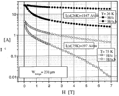
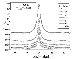
- Pulsed Laser Deposition (PLD) for high-temperature superconductors: Pulsed Laser Deposition is a specialized technique particularly effective for depositing high-temperature superconducting materials. In this process, a high-power laser beam is focused onto a target material, creating a plasma plume that deposits onto a substrate. PLD enables the stoichiometric transfer of complex materials from target to substrate, preserving the composition of multi-element superconductors. This technique allows for precise control of oxygen content, which is critical for oxide-based superconductors. The method is advantageous for research and development due to its flexibility in rapidly changing target materials.
- Post-deposition treatments to enhance superconducting properties: Various post-deposition treatments are employed to optimize the superconducting properties of thin films. These include thermal annealing in controlled atmospheres, oxygen plasma treatments, and ion implantation. Such processes help to improve crystallinity, remove defects, adjust oxygen stoichiometry, and enhance the critical temperature and current density of superconducting films. Post-deposition treatments are essential for activating superconductivity in certain materials and can significantly improve the performance of superconducting devices.
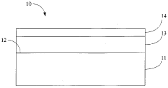
- Substrate selection and preparation for superconducting thin films: The choice and preparation of substrates play a crucial role in the quality of superconducting thin films. Lattice matching between substrate and superconducting material is essential for epitaxial growth and minimizing strain in the films. Common substrates include single-crystal oxides, silicon wafers with buffer layers, and flexible substrates for specific applications. Surface preparation techniques such as chemical cleaning, ion beam etching, and thermal treatment are employed to ensure optimal film adhesion and growth. The substrate temperature during deposition significantly affects the crystallization and microstructure of the superconducting films.
02 Chemical Vapor Deposition (CVD) Methods for Superconductor Fabrication
Chemical vapor deposition techniques offer advantages for creating uniform superconducting thin films over large areas. These methods involve the reaction of precursor gases at the substrate surface to form the desired superconducting compound. Variants include metal-organic CVD (MOCVD) and atomic layer deposition (ALD), which provide excellent control over film stoichiometry and thickness at the atomic level. CVD processes can be optimized to achieve high-temperature superconducting films with superior critical current densities and transition temperatures.Expand Specific Solutions03 Substrate Preparation and Buffer Layer Technologies
The quality of superconducting thin films heavily depends on proper substrate preparation and buffer layer implementation. Various substrate materials including single crystals, biaxially textured metals, and silicon wafers can be used with appropriate buffer layers to promote epitaxial growth of superconducting films. Buffer layers serve multiple purposes: preventing chemical reactions between substrate and superconductor, providing lattice matching, and enabling proper crystallographic orientation of the superconducting layer. Multi-layer buffer architectures can be designed to gradually transition lattice parameters and minimize strain in the superconducting film.Expand Specific Solutions04 Post-Deposition Processing and Annealing Techniques
After thin film deposition, various post-processing techniques are employed to optimize superconducting properties. These include thermal annealing in controlled atmospheres to improve crystallinity, oxygen content adjustment to optimize carrier concentration, and surface passivation to protect against environmental degradation. Rapid thermal annealing and multi-step heat treatment processes can be used to control grain growth and phase formation. These post-deposition treatments significantly enhance critical current density, transition temperature, and overall stability of superconducting films.Expand Specific Solutions05 Novel Materials and Multilayer Structures for Enhanced Superconductivity
Advanced superconducting thin films often incorporate novel materials and multilayer architectures to enhance performance. These include doped compounds, nanocomposites with engineered pinning centers, and superlattice structures with alternating superconducting and non-superconducting layers. Incorporating nanoscale defects and secondary phases can improve flux pinning properties, while heterostructures with normal metals or insulators can be used to create Josephson junctions and other quantum devices. These innovative material systems enable superconducting films with higher critical temperatures, fields, and current densities for practical applications.Expand Specific Solutions
Leading Quantum Device Manufacturers
The thin film deposition of superconductors for quantum devices market is in its growth phase, characterized by increasing investments and technological advancements. The market is expanding rapidly due to rising quantum computing applications, with an estimated value of $500-700 million and projected annual growth of 20-25%. The technology maturity varies across players, with established semiconductor equipment manufacturers like Applied Materials, Lam Research, and Tokyo Electron leading with advanced deposition techniques. Samsung Electronics and Micron Technology are leveraging their semiconductor expertise to develop specialized superconducting thin films. Research-focused entities like American Superconductor and Semiconductor Energy Laboratory are advancing novel materials, while emerging players such as WONIK IPS and Eugene Technology are developing niche solutions for specific quantum device applications.
Samsung Electronics Co., Ltd.
Technical Solution: Samsung Electronics has developed an advanced thin film deposition system for superconducting materials that combines multiple deposition techniques in a single platform. Their system integrates both sputtering and atomic layer deposition capabilities, allowing for versatile fabrication of complex superconductor-based quantum devices. Samsung's technology features a proprietary plasma-enhanced sputtering process that achieves high deposition rates while maintaining film quality. Their system can deposit various superconducting materials including niobium, aluminum, and titanium nitride with thickness control of ±1nm across 300mm wafers. Samsung has implemented advanced process monitoring using in-situ ellipsometry that provides real-time feedback on film growth, enabling precise endpoint detection. For quantum device applications, their platform includes specialized substrate cooling systems that maintain temperatures below 100K during deposition, which helps preserve the superconducting properties of the films. Samsung has also developed custom shadow masking techniques that enable selective area deposition without breaking vacuum, reducing interface contamination in multi-layer quantum circuits.
Strengths: Exceptional integration capabilities for complex multi-material stacks, advanced in-situ monitoring systems, and extensive R&D resources. Weaknesses: Technology primarily optimized for memory and logic applications rather than specifically for quantum devices, potentially requiring adaptation for specialized quantum applications.
Tokyo Electron Ltd.
Technical Solution: Tokyo Electron (TEL) has engineered the Trias™ thin film deposition system specifically optimized for superconducting materials used in quantum computing applications. Their platform utilizes atomic layer deposition (ALD) technology that enables precise control of film thickness at the atomic scale (±0.5Å), which is crucial for maintaining quantum coherence in superconducting qubits. TEL's system features a cryogenic deposition chamber that can operate at temperatures as low as 4K, allowing for the formation of high-quality superconducting films with minimal thermal stress. The platform incorporates proprietary precursor delivery systems that ensure uniform gas distribution across 200mm and 300mm wafers, resulting in exceptional film uniformity. TEL has also developed specialized process recipes for depositing aluminum oxide tunnel barriers with controlled thickness for Josephson junction fabrication, achieving junction resistance variations below 5% across a wafer. Their system includes in-situ surface cleaning capabilities using directed plasma treatment that removes contaminants without damaging the underlying substrate.
Strengths: Industry-leading precision in atomic layer deposition, excellent film uniformity and reproducibility, and integrated multi-step processing capabilities. Weaknesses: Higher operational complexity requiring specialized expertise, and longer processing times compared to some competing technologies.
Breakthrough Patents in Thin Film Superconductivity
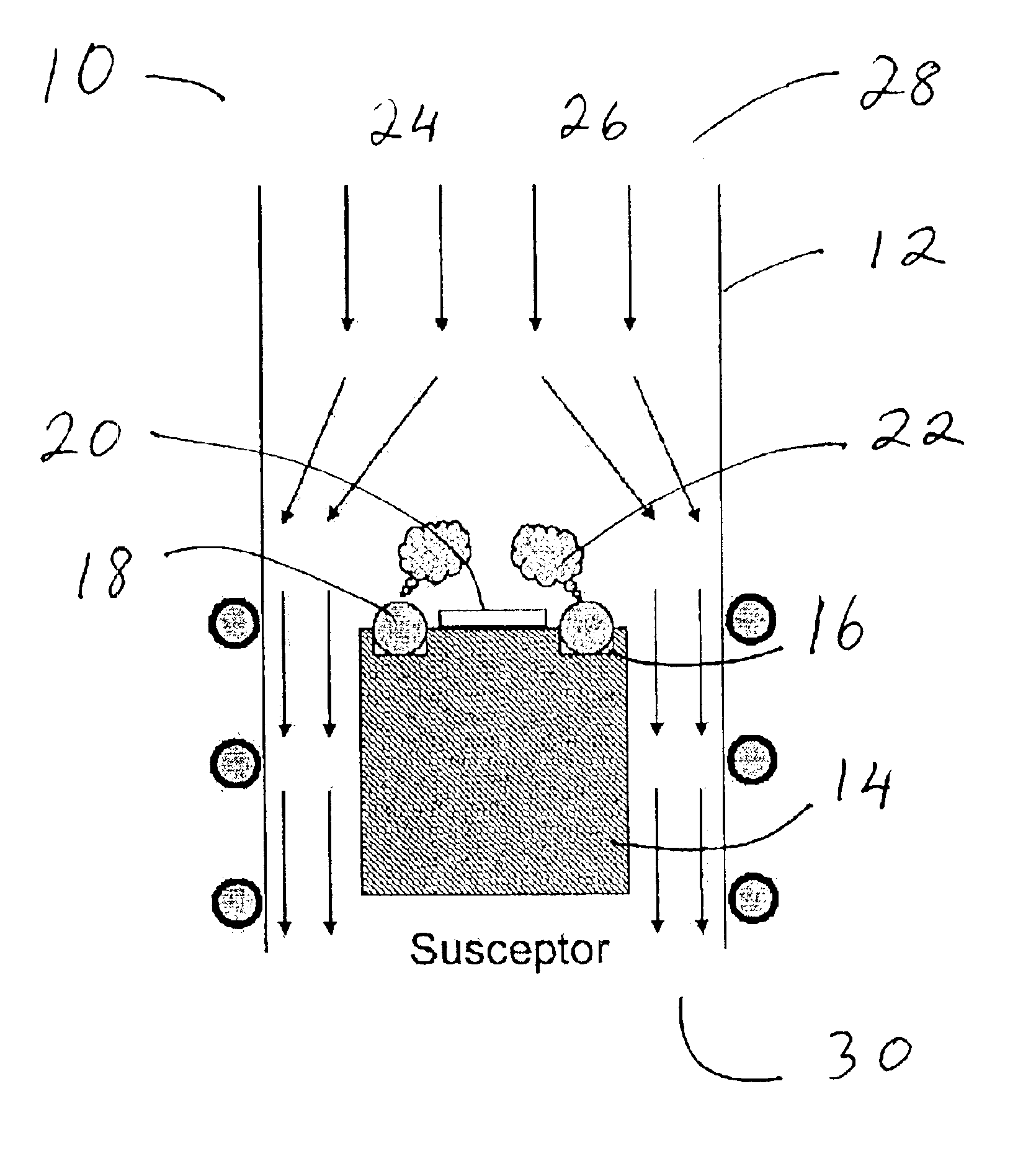
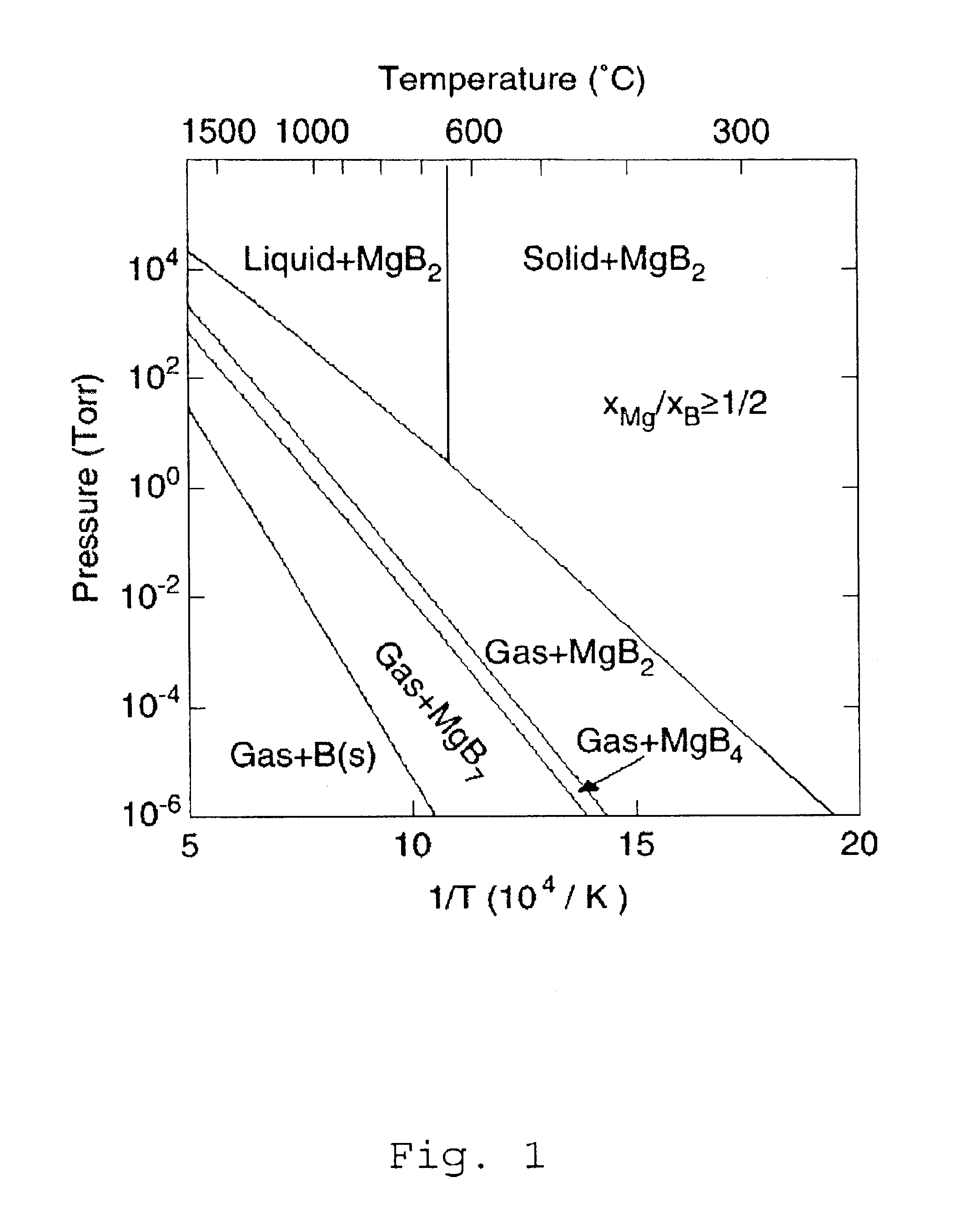
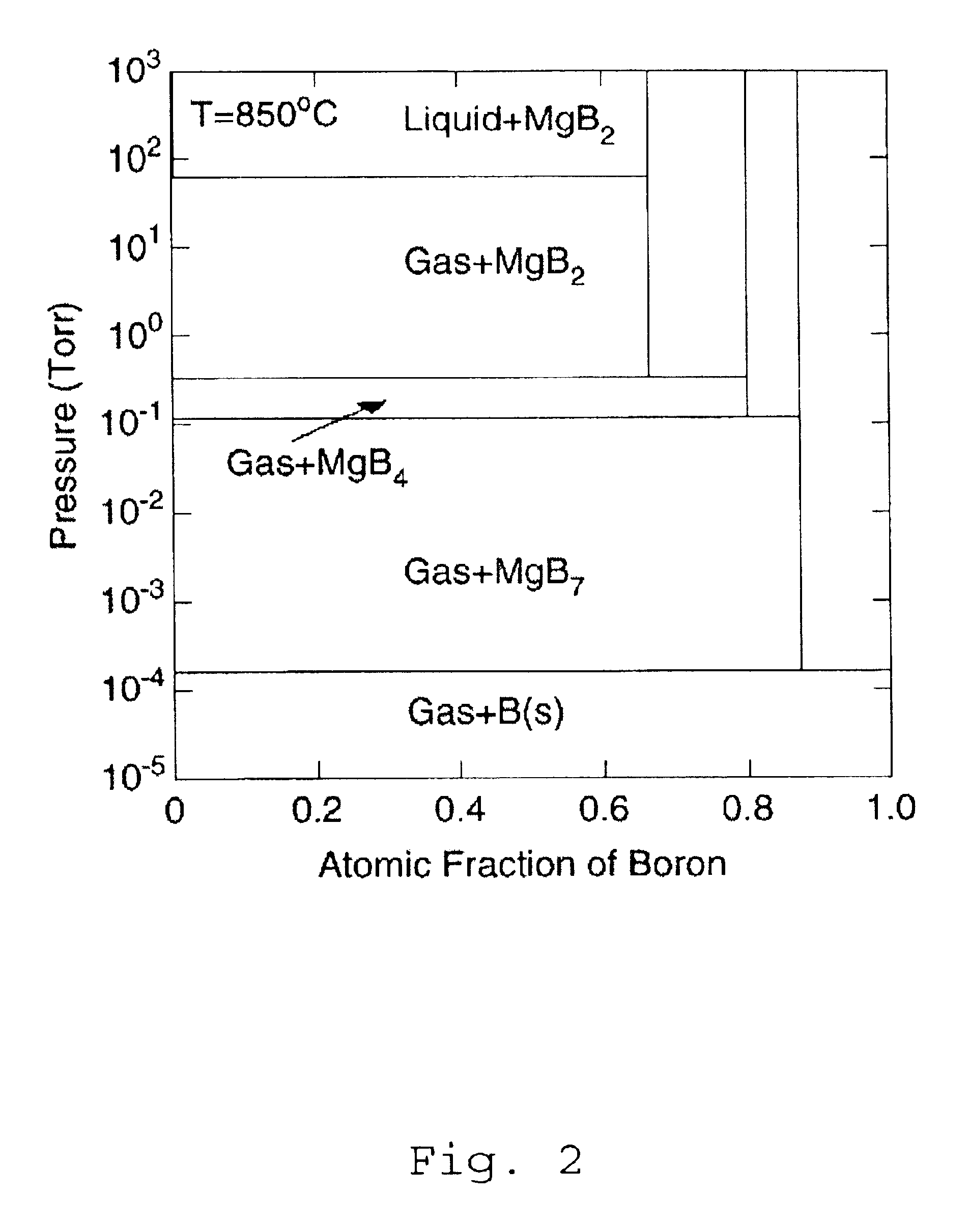
Method for producing boride thin films
PatentInactiveUS6797341B2
Innovation
- A hybrid physical chemical vapor deposition (HPCVD) method combining physical vapor deposition with chemical vapor deposition, using a substrate in a chamber where vapor from a source material like magnesium is generated and combined with a boron-containing precursor, maintaining high Mg partial pressure for thermodynamic stability and epitaxial growth.
Thick superconductor films with improved performance
PatentWO2006137898A2
Innovation
- A low-cost method involving a precursor composition with a fluoride-containing salt, deposited as a solution onto substrates to form a thick superconducting film through thermal processing, where the transition metal to alkaline earth metal ratio is greater than 1.5, and the film thickness is greater than 0.8 μm, using a process that includes heating to form a rare earth-alkaline earth metal-transition metal oxide superconductor.
Cryogenic Infrastructure Requirements
The implementation of superconducting thin films for quantum devices necessitates sophisticated cryogenic infrastructure to maintain operational temperatures well below the critical transition temperature of the superconducting materials. Most quantum computing architectures based on superconducting qubits require temperatures approaching absolute zero, typically in the millikelvin range (10-50 mK), to minimize thermal noise and maintain quantum coherence.
Primary cryogenic systems employed in quantum device operations include dilution refrigerators, which utilize the unique properties of helium-3/helium-4 mixtures to achieve temperatures below 10 mK. These systems represent significant capital investments, often exceeding $500,000 per unit, and require specialized installation environments with minimal vibration and electromagnetic interference.
The operational costs of maintaining cryogenic conditions present substantial ongoing expenses. Liquid helium, the primary coolant, has experienced price volatility and supply constraints globally, with costs ranging from $15-30 per liter depending on geographical location and market conditions. A typical quantum computing facility may consume 100-200 liters weekly, necessitating efficient helium recovery systems to mitigate expenses.
Infrastructure requirements extend beyond refrigeration units to include vibration isolation platforms, electromagnetic shielding, and specialized wiring solutions. Quantum devices are extraordinarily sensitive to environmental perturbations, requiring isolation from mechanical vibrations down to the nanometer scale and electromagnetic shielding capable of attenuating external fields by 60-100 dB across relevant frequency ranges.
Thermal management presents unique challenges in quantum device operation. Superconducting quantum circuits require carefully designed thermal anchoring and filtering of control lines to prevent heat leakage into the cold stage. Each additional control wire introduces a potential thermal pathway, requiring sophisticated filtering solutions that maintain signal integrity while minimizing thermal conductance.
Power infrastructure must accommodate both standard facility requirements and specialized needs for quantum control electronics. Uninterruptible power supplies with conditioning capabilities are essential to prevent system failures during power fluctuations, as thermal cycling of cryogenic systems can introduce significant operational delays (24-72 hours) and potential damage to sensitive components.
Facility design considerations include reinforced flooring (supporting 1000+ kg systems), enhanced HVAC systems for heat dissipation, and dedicated technical gas handling infrastructure. Modern quantum computing facilities increasingly incorporate automated monitoring systems that track cryogenic performance metrics, providing early warning of potential system degradation and optimizing maintenance schedules.
Material Supply Chain Considerations
The superconducting material supply chain for quantum device fabrication presents unique challenges that significantly impact research progress and commercial viability. Rare earth elements and specialized metals such as niobium, aluminum, and tantalum form the foundation of superconducting quantum circuits, with their global distribution concentrated in specific regions. China dominates rare earth element production at approximately 58% of global supply, while niobium reserves are primarily located in Brazil and Canada, creating potential geopolitical vulnerabilities.
Supply chain disruptions, as evidenced during the COVID-19 pandemic, can severely impact research timelines and manufacturing capabilities. The specialized nature of high-purity materials required for quantum applications (99.9999% purity in many cases) further restricts supplier options and increases dependency on specialized vendors. Material costs represent a significant portion of quantum device production expenses, with high-purity substrates like sapphire wafers commanding premium prices compared to standard silicon wafers used in conventional electronics.
Vertical integration strategies are emerging among leading quantum technology companies to secure material supplies. IBM and Google have established dedicated material processing facilities, while others form strategic partnerships with specialized material suppliers. These approaches help mitigate supply risks but require substantial capital investment.
Environmental and regulatory considerations also influence the supply chain landscape. The extraction and processing of rare earth elements often involve environmentally damaging processes, leading to stricter regulations in many jurisdictions. Companies must navigate complex compliance requirements that vary by region, adding another layer of supply chain complexity.
Recycling and material recovery present promising opportunities for supply chain optimization. Advanced recycling techniques for recovering precious metals from decommissioned quantum devices could reduce dependency on primary material sources. Research into alternative materials that maintain necessary quantum properties while utilizing more abundant elements represents another strategic direction for supply chain resilience.
For quantum technology commercialization, establishing robust material supply chains with multiple redundancies is essential. Companies must develop comprehensive supply chain risk management strategies, including geographic diversification of suppliers, strategic stockpiling of critical materials, and investment in alternative material research to ensure long-term viability of quantum device production.
Unlock deeper insights with Patsnap Eureka Quick Research — get a full tech report to explore trends and direct your research. Try now!
Generate Your Research Report Instantly with AI Agent
Supercharge your innovation with Patsnap Eureka AI Agent Platform!