Patents and Industrial Applications of Thin Film Deposition Technologies
SEP 28, 20259 MIN READ
Generate Your Research Report Instantly with AI Agent
Patsnap Eureka helps you evaluate technical feasibility & market potential.
Thin Film Deposition Evolution and Objectives
Thin film deposition technologies have evolved significantly over the past century, transforming from rudimentary vacuum evaporation methods to sophisticated atomic-level precision techniques. The journey began in the early 1900s with thermal evaporation processes, which laid the foundation for modern thin film applications. By the mid-20th century, sputtering techniques emerged, offering improved film quality and substrate adhesion, which revolutionized the electronics industry.
The 1970s witnessed the development of chemical vapor deposition (CVD) methods, enabling the creation of complex multi-layer structures with precise thickness control. This technological advancement coincided with the rapid growth of the semiconductor industry, where thin films became essential components in integrated circuits and microelectronic devices. The subsequent decades saw the refinement of plasma-enhanced CVD and the introduction of atomic layer deposition (ALD), which provided unprecedented control over film composition and thickness at the atomic scale.
Recent advancements have focused on environmentally friendly deposition methods, energy-efficient processes, and techniques compatible with flexible substrates. The integration of computational modeling and artificial intelligence has accelerated the development of novel deposition parameters and material combinations, reducing the traditional trial-and-error approach in process optimization.
The primary objective of thin film deposition technology development has been to achieve precise control over film properties including thickness uniformity, composition, crystallinity, and interface quality. These properties directly influence device performance in applications ranging from microelectronics to optical coatings. Another critical goal has been to increase deposition rates while maintaining quality, thereby improving manufacturing throughput and reducing production costs.
Current research aims to develop deposition technologies capable of creating functional thin films on three-dimensional structures and flexible substrates, which is essential for next-generation electronics and wearable devices. Additionally, there is significant focus on scaling these technologies for industrial production while minimizing environmental impact and resource consumption.
The evolution trajectory suggests that future thin film deposition technologies will likely emphasize atomic precision, in-situ monitoring capabilities, and integration with additive manufacturing techniques. The convergence of these technologies is expected to enable the fabrication of novel materials and structures with tailored properties for specific applications, potentially revolutionizing fields such as energy storage, quantum computing, and biomedical devices.
Market Analysis for Thin Film Applications
The thin film deposition technologies market has experienced robust growth, reaching approximately $70 billion in 2022 with projections to exceed $95 billion by 2027, representing a compound annual growth rate (CAGR) of 6.3%. This growth is primarily driven by increasing demand across multiple industries including semiconductors, optics, energy, and medical devices.
The semiconductor industry remains the largest consumer of thin film technologies, accounting for nearly 45% of the total market share. The continuous miniaturization of electronic components, following Moore's Law, necessitates increasingly sophisticated deposition techniques capable of creating ultra-thin, uniform layers with precise composition control. The transition to 3nm and smaller process nodes has intensified demand for atomic layer deposition (ALD) and advanced physical vapor deposition (PVD) systems.
Renewable energy applications represent the fastest-growing segment, with a CAGR of 9.7%. Thin film solar cells, particularly those utilizing CIGS (copper indium gallium selenide) and perovskite materials, are gaining market traction due to their flexibility, lightweight properties, and improving efficiency-to-cost ratios. The global push toward sustainable energy solutions has created substantial market opportunities in this sector.
The medical and biomedical fields have emerged as significant growth areas, particularly for specialized coatings on implantable devices and biosensors. The market for biocompatible thin films is expected to double within the next five years, driven by innovations in drug delivery systems and tissue engineering applications.
Regionally, Asia-Pacific dominates the market with approximately 58% share, led by manufacturing powerhouses in Taiwan, South Korea, and China. North America follows with 22% market share, distinguished by its focus on R&D and specialized applications in aerospace and defense. Europe accounts for 17% of the market, with particular strength in precision optical coatings and automotive applications.
The competitive landscape features both established equipment manufacturers like Applied Materials, Tokyo Electron, and Lam Research, as well as specialized solution providers focusing on niche applications. Recent market consolidation through mergers and acquisitions indicates a trend toward integrated solution offerings that combine multiple deposition technologies with advanced process control systems.
Customer demands are increasingly centered on sustainability, with growing interest in deposition processes that minimize waste, reduce energy consumption, and eliminate hazardous materials. This shift is creating new market opportunities for equipment manufacturers who can demonstrate environmental advantages alongside traditional performance metrics.
Global Landscape and Technical Barriers
Thin film deposition technologies have evolved significantly across different regions, creating a complex global landscape with varying levels of technological advancement. The United States and Europe have historically dominated patent filings in this domain, with companies like Applied Materials, Lam Research, and ASML holding substantial intellectual property portfolios. However, recent years have witnessed a dramatic shift with East Asian countries, particularly Japan, South Korea, and China, rapidly increasing their patent activities and technological capabilities.
Japan has established itself as a leader in precision deposition techniques, with companies like Tokyo Electron and Canon developing advanced systems for semiconductor manufacturing. South Korea, driven by Samsung and LG, has focused on display-related deposition technologies, particularly for OLED manufacturing. China has made remarkable progress in recent years, with significant investments in both research infrastructure and commercial applications, especially in solar cell manufacturing and consumer electronics.
Despite these advancements, several technical barriers continue to challenge the industry globally. Achieving uniform deposition over large areas remains problematic, particularly as substrate sizes increase for applications like large-area displays and solar panels. The industry struggles with precise thickness control at the atomic level, which becomes increasingly critical for advanced semiconductor nodes below 5nm.
Energy efficiency represents another significant barrier, as many deposition processes require substantial power input, contributing to high manufacturing costs and environmental concerns. The development of low-temperature deposition processes that maintain film quality while reducing thermal budget presents ongoing challenges, especially for temperature-sensitive substrates and devices.
Material compatibility issues persist across different deposition technologies, with certain substrate-film combinations proving difficult to optimize. This is particularly evident in flexible electronics applications, where maintaining film integrity during substrate deformation remains problematic. Additionally, scaling production while maintaining quality and yield presents significant engineering challenges.
The integration of in-situ monitoring and real-time process control represents a frontier that few manufacturers have fully conquered, with most systems still relying on post-deposition characterization rather than dynamic adjustments. Environmental and health concerns related to precursor materials, particularly in chemical vapor deposition processes, have led to regulatory pressures that vary significantly across regions, creating an uneven global development landscape.
Cross-disciplinary barriers also exist, as advances often require expertise spanning materials science, plasma physics, surface chemistry, and mechanical engineering—a combination rarely found within single research groups or companies. These technical challenges, combined with the high capital costs of advanced deposition equipment, have created significant entry barriers that reinforce the dominance of established players in the global market.
Current Deposition Methodologies and Implementations
01 Chemical Vapor Deposition (CVD) Techniques
Chemical Vapor Deposition involves the deposition of thin films through chemical reactions of vapor-phase precursors on a substrate. This technology allows for the creation of high-quality, uniform thin films with excellent step coverage. Various types of CVD processes include thermal CVD, plasma-enhanced CVD (PECVD), and atomic layer deposition (ALD), each offering specific advantages for different applications in semiconductor manufacturing and materials science.- Chemical Vapor Deposition (CVD) Techniques: Chemical Vapor Deposition involves the formation of thin films on substrates through chemical reactions of vapor-phase precursors. This technique allows for the deposition of high-quality, uniform films with excellent step coverage. Various types of CVD processes include thermal CVD, plasma-enhanced CVD (PECVD), and atomic layer deposition (ALD), each offering specific advantages for different applications in semiconductor manufacturing and materials science.
- Physical Vapor Deposition (PVD) Methods: Physical Vapor Deposition encompasses techniques where material is vaporized from a solid or liquid source and transported as vapor through vacuum or plasma environment to the substrate. Common PVD methods include sputtering, evaporation, and pulsed laser deposition. These techniques are widely used for depositing metals, alloys, and some compound materials, offering good control over film thickness and composition without chemical reactions.
- Atomic Layer Deposition (ALD) for Precise Film Control: Atomic Layer Deposition is a specialized thin film deposition technique based on sequential, self-limiting surface reactions. ALD enables precise thickness control at the atomic level, excellent conformality, and uniform deposition on complex geometries. This technique is particularly valuable for creating ultra-thin films, high-k dielectrics, and conformal coatings in advanced semiconductor devices and nanotechnology applications.
- Plasma-Enhanced Deposition Technologies: Plasma-enhanced deposition technologies utilize plasma to activate chemical reactions at lower temperatures than conventional thermal processes. These techniques include plasma-enhanced CVD (PECVD) and plasma-assisted ALD. By using plasma activation, these methods allow for deposition of high-quality films at reduced temperatures, making them suitable for temperature-sensitive substrates and enabling the formation of films with unique properties not achievable through thermal processes alone.
- Equipment and Process Control for Thin Film Deposition: Advanced equipment and process control systems are essential for achieving consistent, high-quality thin film deposition. This includes specialized chambers, gas delivery systems, temperature control mechanisms, and in-situ monitoring tools. Real-time process monitoring and control technologies enable precise adjustment of deposition parameters, ensuring film uniformity, reducing defects, and improving yield in production environments. Innovations in equipment design continue to advance capabilities for complex multi-layer structures and large-area depositions.
02 Physical Vapor Deposition (PVD) Methods
Physical Vapor Deposition encompasses techniques where material is vaporized from a solid or liquid source and transported as vapor through vacuum or plasma environment to the substrate where it condenses. Common PVD methods include sputtering, evaporation, and pulsed laser deposition. These techniques are widely used in manufacturing thin films for electronics, optics, and protective coatings due to their ability to deposit a wide range of materials with precise thickness control.Expand Specific Solutions03 Atomic Layer Deposition (ALD) Systems
Atomic Layer Deposition is a specialized thin film deposition technique based on sequential, self-limiting surface reactions. ALD provides exceptional conformality, precise thickness control at the atomic level, and the ability to deposit uniform films on complex 3D structures. This technology has become increasingly important for manufacturing high-performance semiconductor devices, especially as feature sizes continue to shrink in advanced microelectronics.Expand Specific Solutions04 Plasma-Enhanced Deposition Technologies
Plasma-enhanced deposition technologies utilize plasma to activate chemical reactions at lower temperatures than would otherwise be required. These techniques include plasma-enhanced CVD and plasma-assisted ALD, which enable the deposition of high-quality films on temperature-sensitive substrates. The plasma component enhances reaction rates and allows for better control of film properties, making these methods particularly valuable for manufacturing displays, photovoltaics, and flexible electronics.Expand Specific Solutions05 Equipment and Process Control for Thin Film Deposition
Advanced equipment designs and process control systems are critical for achieving reproducible, high-quality thin film deposition. This includes specialized chambers, gas delivery systems, temperature control mechanisms, and in-situ monitoring tools. Real-time process monitoring and automated control systems help maintain precise deposition parameters, resulting in improved film uniformity, reduced defects, and enhanced manufacturing yield for applications ranging from microelectronics to optical coatings.Expand Specific Solutions
Industry Leaders and Competitive Dynamics
Thin film deposition technologies are currently in a mature growth phase, with the global market estimated at $70 billion and expanding at 8-10% annually. The competitive landscape features established semiconductor equipment manufacturers like Applied Materials, Tokyo Electron, and ASM IP Holding, alongside diversified technology corporations such as Samsung Electronics and IBM. Major semiconductor manufacturers including TSMC, Samsung Display, and Micron Technology are driving innovation through vertical integration. The technology has reached commercial maturity in semiconductor applications, with companies now focusing on specialized applications in optics (Nikon, Eastman Kodak), renewable energy (First Solar), and advanced materials. Research institutions like Harvard, North Carolina State University, and the Institute of Microelectronics of Chinese Academy of Sciences are pioneering next-generation deposition techniques, indicating continued evolution of this foundational technology.
SAMSUNG DISPLAY CO LTD
Technical Solution: Samsung Display has developed specialized thin film deposition technologies optimized for advanced display manufacturing. Their portfolio includes large-area PECVD systems for TFT backplanes and encapsulation layers in OLED displays. Samsung has pioneered advanced organic thin film deposition techniques using Linear Source Deposition (LSD) technology that achieves exceptional uniformity across Gen 8.5+ substrates[6]. Their vacuum thermal evaporation systems for OLED manufacturing feature sophisticated shadow mask technologies that enable side-by-side RGB patterning with micron-level precision. Samsung has developed specialized thin film encapsulation (TFE) technology that combines inorganic barrier layers deposited by PECVD with organic layers to achieve water vapor transmission rates below 10^-6 g/m²/day, critical for flexible OLED longevity. Their oxide semiconductor deposition technology creates high-mobility IGZO films for advanced TFTs with mobility exceeding 10 cm²/Vs. Samsung has also developed specialized deposition processes for quantum dot color conversion layers used in their QD-OLED displays, combining vacuum deposition with solution processing techniques to achieve precise patterning of quantum dot materials.
Strengths: Unparalleled expertise in large-area deposition for display applications; advanced organic material deposition capabilities; sophisticated integration of multiple thin film technologies in complex display stacks. Weaknesses: Technologies primarily optimized for display applications rather than broader semiconductor use; high material consumption in some evaporation processes; challenges in scaling certain technologies to larger substrate sizes.
Applied Materials, Inc.
Technical Solution: Applied Materials has developed advanced thin film deposition technologies including Physical Vapor Deposition (PVD), Chemical Vapor Deposition (CVD), Atomic Layer Deposition (ALD), and Epitaxial Deposition systems. Their flagship Endura® platform integrates multiple PVD chambers for complex semiconductor manufacturing, enabling precise deposition of materials at atomic scale. The company's Producer® platform for CVD processes allows for uniform thin film deposition across large substrates with exceptional thickness control. Applied Materials has pioneered selective deposition techniques that can deposit materials only where needed, reducing process steps and improving device performance. Their ALD technology achieves conformal films as thin as a few angstroms with precise thickness control for high-aspect-ratio structures in advanced logic and memory devices[1][3]. Recent innovations include their Integrated Materials Solution for interconnect applications that combines PVD, CVD, and ALD in a single platform to address critical challenges in copper interconnect scaling.
Strengths: Industry-leading equipment portfolio covering virtually all thin film deposition methods; extensive process expertise across multiple materials systems; strong integration capabilities allowing for multi-step deposition sequences without vacuum break. Weaknesses: High capital equipment costs; complex systems require significant technical expertise to operate and maintain; some technologies have high operational costs due to precursor materials and energy consumption.
Key Patents and Technical Innovations
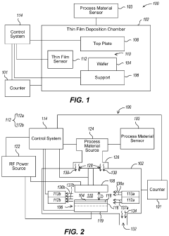
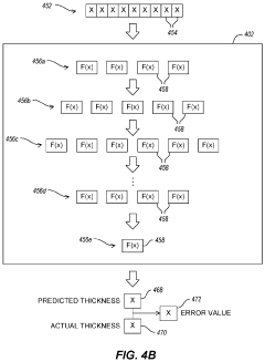
Method and system for adjusting location of a wafer and a top plate in a thin-film deposition process
PatentActiveUS12014910B2
Innovation
- A thin-film deposition system that includes sensors to monitor the gap and thin-film characteristics, with a control system that adjusts the relative location of the top plate and wafer in situ during the deposition process to maintain optimal gap sizes and ensure uniform deposition rates.
Materials Science Advancements and Compatibility
The evolution of thin film deposition technologies has been significantly influenced by advancements in materials science. Recent breakthroughs in material compatibility have expanded the application scope of these technologies across multiple industries. Traditional deposition methods often faced limitations when working with temperature-sensitive substrates or when attempting to create multi-material structures. However, modern techniques have overcome many of these challenges through innovative approaches to material interaction and interface engineering.
Materials science research has enabled the development of precursors specifically designed for atomic layer deposition (ALD) and chemical vapor deposition (CVD) processes. These precursors demonstrate enhanced reactivity at lower temperatures, allowing for deposition on thermally sensitive substrates such as polymers and biological materials. This advancement has been particularly valuable in flexible electronics and biomedical device manufacturing, where traditional high-temperature processes would damage the underlying materials.
Significant progress has also been made in understanding and controlling the crystallization behavior of thin films during deposition. By manipulating process parameters such as temperature gradients, pressure conditions, and deposition rates, researchers have achieved precise control over film microstructure. This control enables the tailoring of material properties including electrical conductivity, optical transparency, and mechanical durability to meet specific application requirements.
Interface engineering represents another critical area of materials science advancement in thin film technology. The development of adhesion layers and buffer materials has solved many of the compatibility issues that previously limited multi-material integration. Patents in this domain frequently address novel interlayer materials that facilitate strong bonding between dissimilar materials while preventing unwanted diffusion or chemical reactions at interfaces.
Nanoscale material design has further revolutionized thin film capabilities. The incorporation of nanostructured materials, such as quantum dots, nanowires, and two-dimensional materials like graphene, has introduced unprecedented functional properties to thin films. These materials enable enhanced performance in applications ranging from photovoltaics to sensing technologies, with recent patents focusing on scalable methods for their integration into conventional thin film manufacturing processes.
Environmental considerations have also driven materials compatibility research, with significant effort directed toward developing non-toxic alternatives to traditional materials used in thin film deposition. Lead-free piezoelectrics, cadmium-free quantum dots, and halogen-free flame retardants represent important advances that maintain performance while reducing environmental impact, addressing both regulatory requirements and sustainability goals in industrial applications.
Environmental Impact and Sustainability Considerations
Thin film deposition technologies, while offering significant technological advantages, present notable environmental challenges that must be addressed for sustainable industrial implementation. The environmental footprint of these processes encompasses energy consumption, resource utilization, waste generation, and potential emissions of hazardous substances. Traditional deposition methods such as Physical Vapor Deposition (PVD) and Chemical Vapor Deposition (CVD) often require substantial energy inputs, with vacuum systems and high-temperature processes contributing significantly to carbon emissions.
Material efficiency represents another critical environmental concern, as many deposition processes utilize rare or toxic precursors with low deposition efficiency rates. The semiconductor industry, for instance, reports material utilization rates below 30% for certain PVD processes, resulting in significant waste generation. Additionally, precursor chemicals like perfluorocompounds (PFCs) used in plasma-enhanced CVD contribute to global warming with greenhouse potential thousands of times greater than CO2.
Recent patent activities demonstrate increasing focus on environmentally responsible deposition technologies. Notable innovations include closed-loop precursor recycling systems, energy-efficient plasma sources, and room-temperature deposition techniques. Patent US10876236B2 describes a sustainable ALD process utilizing non-toxic precursors, while EP3456844A1 presents energy-efficient pulsed magnetron sputtering technology reducing power consumption by up to 40%.
Industry sustainability initiatives are gaining momentum, with major manufacturers implementing green manufacturing principles. Companies like Applied Materials and Tokyo Electron have developed equipment with reduced environmental impact, including systems with improved material utilization and decreased energy requirements. The adoption of lifecycle assessment methodologies has become increasingly prevalent, enabling comprehensive evaluation of environmental impacts from raw material extraction through end-of-life considerations.
Regulatory frameworks worldwide are evolving to address environmental concerns associated with thin film technologies. The European Union's REACH regulation and RoHS directive have significantly influenced material selection in deposition processes, driving innovation toward less hazardous alternatives. Similarly, emissions standards in various jurisdictions have prompted development of advanced abatement systems for process effluents, with recent patents focusing on point-of-use treatment technologies for perfluorinated compounds and volatile organic compounds.
Looking forward, sustainable thin film deposition represents both a challenge and opportunity for industrial innovation. Emerging approaches such as solution-based deposition methods, biomimetic processes, and ambient-condition techniques offer promising pathways toward environmentally responsible manufacturing while maintaining the performance characteristics essential for advanced applications.
Unlock deeper insights with Patsnap Eureka Quick Research — get a full tech report to explore trends and direct your research. Try now!
Generate Your Research Report Instantly with AI Agent
Supercharge your innovation with Patsnap Eureka AI Agent Platform!