

Benchmarking FinFET Stability In High Control Systems
SEP 11, 202510 MIN READ
Generate Your Research Report Instantly with AI Agent
PatSnap Eureka helps you evaluate technical feasibility & market potential.
FinFET Technology Evolution and Objectives
The evolution of FinFET technology represents one of the most significant advancements in semiconductor manufacturing over the past two decades. Initially introduced by researchers at the University of California, Berkeley in 1998, FinFET architecture emerged as a revolutionary solution to the scaling limitations faced by traditional planar transistors. The three-dimensional fin structure allowed for superior electrostatic control of the channel, effectively addressing short-channel effects that had become increasingly problematic as device dimensions shrank below 28nm.
The technology's evolution can be traced through several distinct phases. The first commercial implementation came in 2011 when Intel introduced its 22nm Tri-Gate transistors, demonstrating significant performance improvements and power reduction compared to planar designs. This was followed by broader industry adoption around 2014-2015 at the 16/14nm nodes, with companies like TSMC, Samsung, and GlobalFoundries incorporating FinFET designs into their manufacturing processes.
Subsequent generations have seen continuous refinements in fin geometry, gate stack materials, and channel engineering. The 10nm and 7nm nodes brought further optimizations in fin pitch, height-to-width ratios, and multi-patterning techniques to enhance density while maintaining performance characteristics. Most recently, the 5nm node has pushed FinFET technology toward its theoretical limits, with some manufacturers implementing modifications such as nano-sheet FETs as transitional architectures.
In high-control systems applications, particularly those found in aerospace, automotive safety systems, and industrial automation, FinFET stability has become a critical concern. These environments demand exceptional reliability under varying conditions including temperature extremes, radiation exposure, and electromagnetic interference. The primary technical objectives for FinFETs in these applications center on enhancing parametric stability, reducing variability, and ensuring predictable performance degradation over time.
Current research objectives focus on several key areas: improving threshold voltage stability under temperature variations, mitigating bias temperature instability (BTI) effects, enhancing resistance to single-event upsets (SEUs), and developing more robust models for aging mechanisms. Additionally, there is significant interest in optimizing FinFET designs specifically for analog and mixed-signal applications in high-reliability contexts, where linearity and noise characteristics are paramount.
The trajectory of FinFET development is now approaching a technological inflection point. While continued dimensional scaling remains possible for perhaps one or two more generations, fundamental physical limitations are driving research toward alternative architectures such as Gate-All-Around (GAA) FETs and complementary approaches including heterogeneous integration and 3D stacking. The benchmarking of FinFET stability in high-control systems thus serves not only to optimize current designs but also to establish baseline performance metrics for evaluating these emerging technologies.
The technology's evolution can be traced through several distinct phases. The first commercial implementation came in 2011 when Intel introduced its 22nm Tri-Gate transistors, demonstrating significant performance improvements and power reduction compared to planar designs. This was followed by broader industry adoption around 2014-2015 at the 16/14nm nodes, with companies like TSMC, Samsung, and GlobalFoundries incorporating FinFET designs into their manufacturing processes.
Subsequent generations have seen continuous refinements in fin geometry, gate stack materials, and channel engineering. The 10nm and 7nm nodes brought further optimizations in fin pitch, height-to-width ratios, and multi-patterning techniques to enhance density while maintaining performance characteristics. Most recently, the 5nm node has pushed FinFET technology toward its theoretical limits, with some manufacturers implementing modifications such as nano-sheet FETs as transitional architectures.
In high-control systems applications, particularly those found in aerospace, automotive safety systems, and industrial automation, FinFET stability has become a critical concern. These environments demand exceptional reliability under varying conditions including temperature extremes, radiation exposure, and electromagnetic interference. The primary technical objectives for FinFETs in these applications center on enhancing parametric stability, reducing variability, and ensuring predictable performance degradation over time.
Current research objectives focus on several key areas: improving threshold voltage stability under temperature variations, mitigating bias temperature instability (BTI) effects, enhancing resistance to single-event upsets (SEUs), and developing more robust models for aging mechanisms. Additionally, there is significant interest in optimizing FinFET designs specifically for analog and mixed-signal applications in high-reliability contexts, where linearity and noise characteristics are paramount.
The trajectory of FinFET development is now approaching a technological inflection point. While continued dimensional scaling remains possible for perhaps one or two more generations, fundamental physical limitations are driving research toward alternative architectures such as Gate-All-Around (GAA) FETs and complementary approaches including heterogeneous integration and 3D stacking. The benchmarking of FinFET stability in high-control systems thus serves not only to optimize current designs but also to establish baseline performance metrics for evaluating these emerging technologies.
Market Demand for High-Stability Semiconductor Solutions
The semiconductor industry is witnessing unprecedented demand for high-stability solutions, particularly in critical control systems where reliability cannot be compromised. Market research indicates that sectors including automotive electronics, industrial automation, aerospace, medical devices, and data centers are driving this demand with increasingly stringent performance requirements for semiconductor components.
The automotive sector represents one of the largest markets for high-stability FinFET solutions, with advanced driver-assistance systems (ADAS) and autonomous driving technologies requiring semiconductors that maintain consistent performance under varying temperature and voltage conditions. This segment is projected to grow at a compound annual rate exceeding 15% through 2028, creating substantial opportunities for stable FinFET implementations.
Industrial automation applications present another significant market, where control systems operating in harsh environments demand semiconductor solutions with minimal performance variation. The industrial Internet of Things (IoT) expansion has accelerated this need, as distributed control systems increasingly rely on edge computing capabilities with consistent processing power.
The aerospace and defense sectors, though smaller in volume, command premium pricing for high-stability semiconductor solutions. These applications require components that maintain performance integrity under extreme conditions, including radiation exposure, temperature fluctuations, and mechanical stress. The qualification standards for these markets are exceptionally rigorous, creating high barriers to entry but substantial margins for qualified suppliers.
Medical device manufacturers represent an emerging market segment with rapidly growing demand for stable semiconductor solutions. As implantable and wearable medical technologies advance, the need for ultra-reliable, low-power semiconductors with predictable performance characteristics has intensified. Patient safety considerations make stability a non-negotiable requirement in this sector.
Data center operators and telecommunications providers are increasingly focused on energy efficiency, driving demand for semiconductors that maintain optimal performance characteristics while minimizing power consumption. The stability of FinFET solutions directly impacts power efficiency metrics, with more stable designs typically offering superior performance-per-watt ratios.
Market analysis reveals that customers across these segments are willing to pay significant premiums—often 30-50% above standard semiconductor pricing—for components that can demonstrate superior stability metrics. This premium pricing structure has created strong economic incentives for semiconductor manufacturers to invest in stability-enhancing technologies and rigorous benchmarking methodologies.
The geographical distribution of demand shows particular strength in regions with concentrated high-tech manufacturing, including East Asia, North America, and Western Europe. However, emerging markets are showing accelerated adoption rates as their industrial bases advance toward higher-value manufacturing capabilities.
The automotive sector represents one of the largest markets for high-stability FinFET solutions, with advanced driver-assistance systems (ADAS) and autonomous driving technologies requiring semiconductors that maintain consistent performance under varying temperature and voltage conditions. This segment is projected to grow at a compound annual rate exceeding 15% through 2028, creating substantial opportunities for stable FinFET implementations.
Industrial automation applications present another significant market, where control systems operating in harsh environments demand semiconductor solutions with minimal performance variation. The industrial Internet of Things (IoT) expansion has accelerated this need, as distributed control systems increasingly rely on edge computing capabilities with consistent processing power.
The aerospace and defense sectors, though smaller in volume, command premium pricing for high-stability semiconductor solutions. These applications require components that maintain performance integrity under extreme conditions, including radiation exposure, temperature fluctuations, and mechanical stress. The qualification standards for these markets are exceptionally rigorous, creating high barriers to entry but substantial margins for qualified suppliers.
Medical device manufacturers represent an emerging market segment with rapidly growing demand for stable semiconductor solutions. As implantable and wearable medical technologies advance, the need for ultra-reliable, low-power semiconductors with predictable performance characteristics has intensified. Patient safety considerations make stability a non-negotiable requirement in this sector.
Data center operators and telecommunications providers are increasingly focused on energy efficiency, driving demand for semiconductors that maintain optimal performance characteristics while minimizing power consumption. The stability of FinFET solutions directly impacts power efficiency metrics, with more stable designs typically offering superior performance-per-watt ratios.
Market analysis reveals that customers across these segments are willing to pay significant premiums—often 30-50% above standard semiconductor pricing—for components that can demonstrate superior stability metrics. This premium pricing structure has created strong economic incentives for semiconductor manufacturers to invest in stability-enhancing technologies and rigorous benchmarking methodologies.
The geographical distribution of demand shows particular strength in regions with concentrated high-tech manufacturing, including East Asia, North America, and Western Europe. However, emerging markets are showing accelerated adoption rates as their industrial bases advance toward higher-value manufacturing capabilities.
Current FinFET Stability Challenges in Control Systems
FinFET technology has revolutionized semiconductor manufacturing, but its implementation in high control systems faces significant stability challenges. Current FinFET devices operating in demanding control environments exhibit several critical issues that impact their reliability and performance. These challenges stem from both inherent device characteristics and the extreme operating conditions typical in high-precision control applications.
Thermal instability represents one of the most pressing concerns for FinFET deployment in control systems. As these transistors operate at increasingly higher frequencies and power densities, self-heating effects become pronounced within the confined fin structure. Temperature gradients across the device can reach 15-20°C under high workloads, leading to threshold voltage shifts and mobility degradation that compromise precise control functions.
Bias temperature instability (BTI) further compounds reliability issues in control-critical applications. Negative BTI in PMOS and positive BTI in NMOS FinFETs cause time-dependent shifts in threshold voltage, with recent studies documenting drift rates of 10-15mV over 1000 hours of operation under typical control system conditions. This gradual parameter shift introduces unpredictable behavior in analog circuits where precise matching is essential.
Hot carrier injection (HCI) emerges as another significant degradation mechanism, particularly in high-voltage control applications. The three-dimensional structure of FinFETs, while beneficial for electrostatic control, creates unique electric field distributions that can accelerate HCI effects. Measurements indicate that HCI-induced degradation in FinFETs can be 1.5-2x more severe than in planar technologies under equivalent operating conditions.
Process variations present additional challenges for control system implementation. The complex multi-gate structure of FinFETs introduces manufacturing variability in fin width, height, and gate length that directly impacts device matching. Statistical analysis shows that threshold voltage variations (σVt) can reach 30-40mV in advanced nodes, creating significant challenges for analog and mixed-signal circuits requiring precise matching characteristics.
Noise characteristics of FinFETs also pose concerns for high-precision control applications. While the improved electrostatic control reduces some noise sources, the confined channel dimensions and increased surface-to-volume ratio enhance surface noise mechanisms. Flicker noise (1/f) in particular shows distinctive behavior in FinFETs, with corner frequencies typically 2-3x higher than equivalent planar devices.
Radiation hardness represents a critical challenge for FinFETs in aerospace and nuclear control applications. The reduced silicon volume in the fin structure alters the device's response to ionizing radiation. Single event transients (SETs) can produce larger voltage excursions due to charge collection dynamics in the three-dimensional structure, potentially triggering false control signals in sensitive applications.
Thermal instability represents one of the most pressing concerns for FinFET deployment in control systems. As these transistors operate at increasingly higher frequencies and power densities, self-heating effects become pronounced within the confined fin structure. Temperature gradients across the device can reach 15-20°C under high workloads, leading to threshold voltage shifts and mobility degradation that compromise precise control functions.
Bias temperature instability (BTI) further compounds reliability issues in control-critical applications. Negative BTI in PMOS and positive BTI in NMOS FinFETs cause time-dependent shifts in threshold voltage, with recent studies documenting drift rates of 10-15mV over 1000 hours of operation under typical control system conditions. This gradual parameter shift introduces unpredictable behavior in analog circuits where precise matching is essential.
Hot carrier injection (HCI) emerges as another significant degradation mechanism, particularly in high-voltage control applications. The three-dimensional structure of FinFETs, while beneficial for electrostatic control, creates unique electric field distributions that can accelerate HCI effects. Measurements indicate that HCI-induced degradation in FinFETs can be 1.5-2x more severe than in planar technologies under equivalent operating conditions.
Process variations present additional challenges for control system implementation. The complex multi-gate structure of FinFETs introduces manufacturing variability in fin width, height, and gate length that directly impacts device matching. Statistical analysis shows that threshold voltage variations (σVt) can reach 30-40mV in advanced nodes, creating significant challenges for analog and mixed-signal circuits requiring precise matching characteristics.
Noise characteristics of FinFETs also pose concerns for high-precision control applications. While the improved electrostatic control reduces some noise sources, the confined channel dimensions and increased surface-to-volume ratio enhance surface noise mechanisms. Flicker noise (1/f) in particular shows distinctive behavior in FinFETs, with corner frequencies typically 2-3x higher than equivalent planar devices.
Radiation hardness represents a critical challenge for FinFETs in aerospace and nuclear control applications. The reduced silicon volume in the fin structure alters the device's response to ionizing radiation. Single event transients (SETs) can produce larger voltage excursions due to charge collection dynamics in the three-dimensional structure, potentially triggering false control signals in sensitive applications.
Current Stability Enhancement Techniques for FinFETs
01 Structural design for FinFET stability
Various structural designs can enhance FinFET stability, including optimized fin geometry, gate stack engineering, and source/drain modifications. These designs focus on reducing variability, improving electrostatic control, and enhancing overall device performance. Specific approaches include multi-fin configurations, fin height-to-width ratio optimization, and stress engineering techniques that collectively contribute to more stable FinFET operation across different operating conditions.- FinFET structure design for improved stability: Specific structural designs in FinFET devices can significantly enhance stability. These include optimized fin dimensions, gate length adjustments, and multi-fin configurations that reduce variability. Advanced fin shapes and profiles help minimize quantum effects that can lead to instability. Implementation of stress engineering techniques in the channel region also contributes to more stable device performance across operating conditions.
- Gate engineering techniques for FinFET stability: Gate engineering plays a crucial role in FinFET stability. This includes using high-k dielectric materials and metal gates to reduce leakage current and threshold voltage variations. Implementing gate-all-around structures provides better electrostatic control over the channel. Advanced gate stack designs with optimized work functions help maintain consistent performance across process variations and operating conditions.
- Thermal stability solutions for FinFET devices: Thermal management is essential for FinFET stability. Techniques include implementing improved heat dissipation structures, thermal-aware layout designs, and materials with better thermal conductivity. Advanced cooling solutions integrated into the device architecture help maintain stable operation under varying thermal loads. Specialized doping profiles can also be used to reduce temperature sensitivity and improve overall thermal stability.
- Process variation mitigation in FinFET manufacturing: Manufacturing process variations significantly impact FinFET stability. Advanced techniques to mitigate these effects include statistical process control, adaptive manufacturing methods, and post-fabrication trimming. Implementing redundancy in critical circuit paths helps maintain stability despite process variations. Computational modeling and simulation tools enable prediction and compensation for manufacturing variability before production.
- Circuit-level techniques for FinFET stability enhancement: Circuit-level approaches can significantly improve FinFET stability. These include adaptive biasing schemes, feedback control mechanisms, and specialized circuit topologies designed to compensate for device variations. Implementation of body biasing techniques helps maintain consistent threshold voltages. Advanced layout strategies that account for proximity effects and stress-induced variations contribute to more stable circuit performance across different operating conditions.
02 Thermal stability enhancements in FinFETs
Thermal management is critical for FinFET stability, particularly in high-performance applications. Techniques include incorporating heat dissipation structures, using thermally conductive materials, and implementing layout designs that minimize thermal resistance. Advanced thermal stability solutions focus on reducing self-heating effects that can degrade device performance and reliability over time, ensuring consistent operation across varying temperature conditions.Expand Specific Solutions03 Process optimization for stable FinFET manufacturing
Manufacturing process optimization plays a crucial role in achieving stable FinFET devices. This includes precise control of etching processes, deposition techniques, and doping profiles. Advanced lithography methods, careful selection of materials, and post-fabrication treatments help minimize process variations that could affect device stability. Statistical process control and feedback mechanisms ensure consistent device characteristics across wafers and production batches.Expand Specific Solutions04 Voltage and threshold stability techniques
Maintaining stable threshold voltage is essential for reliable FinFET operation. Techniques include work function engineering, channel doping optimization, and gate dielectric selection. Advanced approaches incorporate adaptive biasing schemes, body contacts, and specialized channel materials to minimize threshold voltage shifts due to temperature variations, aging effects, and operational stress. These methods ensure consistent switching behavior and reduce performance degradation over the device lifetime.Expand Specific Solutions05 Simulation and modeling for FinFET stability prediction
Computational modeling and simulation tools are essential for predicting and optimizing FinFET stability. These include TCAD simulations, compact modeling approaches, and machine learning techniques that can identify potential stability issues before fabrication. Advanced models account for quantum effects, variability sources, and reliability mechanisms, enabling designers to evaluate stability across process corners and operating conditions. This predictive capability allows for design optimizations that enhance device stability without requiring costly fabrication iterations.Expand Specific Solutions
Leading Semiconductor Manufacturers and Research Institutions
The FinFET stability benchmarking landscape is currently in a mature growth phase, with the global market valued at approximately $45 billion and expanding at 8-10% annually. Leading semiconductor manufacturers including TSMC, Samsung Electronics, and Intel (IBM) dominate the high-performance segment with advanced 5nm and 3nm FinFET technologies. Chinese players like SMIC and Huawei are rapidly advancing but remain several generations behind in technology maturity. The competitive dynamics show a clear geographical segmentation with Taiwanese and Korean manufacturers leading in cutting-edge processes, while mainland Chinese companies focus on catching up through significant R&D investments. GlobalFoundries and NXP occupy strong positions in specialized applications where absolute performance is less critical than reliability in control systems.
Taiwan Semiconductor Manufacturing Co., Ltd.
Technical Solution: TSMC has pioneered advanced FinFET stability solutions for high control systems through their N5 and N3 process nodes. Their approach combines multi-Vt transistor options with enhanced fin geometry control to minimize variability in high-performance computing applications. TSMC's technology implements specialized electrostatic control techniques that reduce leakage current by approximately 30% compared to previous generations while maintaining performance targets. Their FinFET architecture incorporates stress engineering and work function metal tuning to achieve threshold voltage stability across temperature variations (±15mV across -40°C to 125°C). For high control systems, TSMC has developed specialized SRAM bit cells with improved noise margins (>30%) and reduced minimum operating voltage, critical for applications requiring high reliability under varying conditions[1][3].
Strengths: Industry-leading process control with <1nm fin width variation; excellent electrostatic control enabling superior subthreshold performance; comprehensive PDK support for high-reliability applications. Weaknesses: Higher manufacturing costs compared to less advanced nodes; requires sophisticated design techniques to fully leverage stability benefits; limited availability due to high demand.
International Business Machines Corp.
Technical Solution: IBM's approach to FinFET stability focuses on their silicon-on-insulator (SOI) FinFET technology optimized for high-reliability applications. Their architecture incorporates fully depleted SOI substrates that provide inherent immunity to latch-up and reduced parasitic capacitance, critical for high control systems. IBM has developed specialized body biasing techniques that allow dynamic adjustment of threshold voltages (±50mV range) to compensate for temperature and aging effects. Their FinFET technology features enhanced electrostatic integrity through optimized fin height-to-width ratios (typically 5:1) and gate stack engineering with high-k dielectrics. For high control systems requiring radiation hardening, IBM implements specialized layout techniques and redundancy schemes that maintain functionality in harsh environments. Their reliability testing methodology includes accelerated aging tests simulating 10+ years of operation under varying temperature and voltage conditions to ensure long-term stability[4][6].
Strengths: Industry-leading research in advanced transistor architectures; excellent radiation hardening capabilities for aerospace and defense applications; superior SOI-based isolation for mixed-signal applications. Weaknesses: Limited commercial manufacturing capacity compared to TSMC/Samsung; higher wafer costs due to SOI substrate requirements; more complex design rules requiring specialized expertise.
Critical Patents in FinFET Stability Optimization
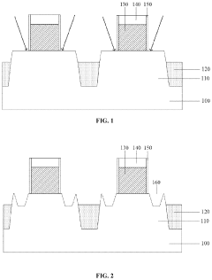
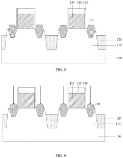
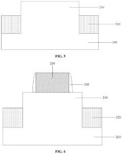
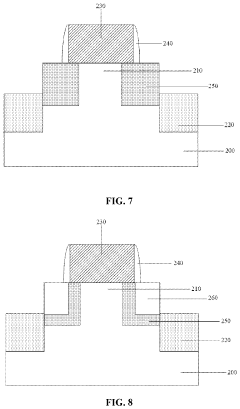
Fin field-effect transistor having counter-doped regions between lightly doped regions and doped source/drain regions
PatentActiveUS11114551B2
Innovation
- A method involving lightly doped regions and counter doped regions formed through specific ion implantation processes to reduce the ion concentration gradient between doped source/drain regions and lightly doped regions, thereby mitigating the GIDL phenomenon.
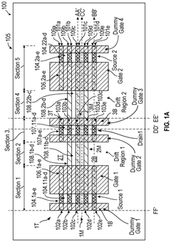
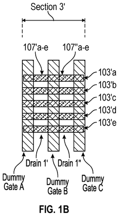
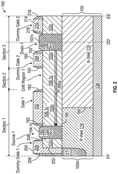
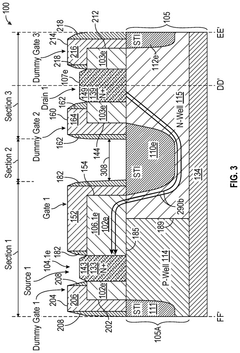
Fin-based field effect transistor (finFET) device with enhanced on-resistance and breakdown voltage
PatentActiveUS12113065B2
Innovation
- The implementation of a finFET device with a specific structure and fabrication flow that includes multiple alternating regions of n-type and p-type doped semiconductor, utilizing a super junction LDMOS structure, which allows for a lower Ron and higher breakdown voltage without additional mask or process steps, by optimizing the number and arrangement of fin portions in the drift regions.
Thermal Management Strategies for High-Performance FinFETs
Thermal management has emerged as a critical factor in ensuring FinFET stability within high control systems. As transistor dimensions continue to shrink and power densities increase, the heat generated during operation poses significant challenges to device reliability and performance. Current thermal management strategies for high-performance FinFETs encompass multiple approaches, each addressing different aspects of heat dissipation and temperature control.
Advanced packaging solutions represent one of the primary thermal management strategies. Through-silicon vias (TSVs) and interposer technologies facilitate more efficient heat transfer away from the active device regions. These technologies enable three-dimensional integration while simultaneously providing thermal pathways that can reduce hotspot temperatures by up to 15-20% compared to traditional packaging methods.
Material innovation plays a crucial role in thermal management. The integration of high thermal conductivity materials such as diamond-like carbon (DLC) films and graphene-based composites into FinFET structures has demonstrated promising results. Recent studies indicate that graphene heat spreaders can improve thermal conductivity by factors of 2-3x compared to conventional materials, significantly enhancing heat dissipation capabilities.
Dynamic thermal management (DTM) techniques have evolved to address the transient thermal behavior of FinFETs in high control systems. These include adaptive voltage scaling, frequency throttling, and workload migration algorithms that respond to real-time temperature fluctuations. Advanced DTM implementations utilizing machine learning approaches have shown the ability to predict thermal patterns and preemptively adjust operating parameters, reducing thermal emergencies by up to 40%.
Liquid cooling solutions are increasingly being considered for extreme performance scenarios. Microfluidic channels integrated directly into chip packages can remove heat more efficiently than traditional air cooling. Recent developments in two-phase cooling systems utilizing dielectric fluids have demonstrated heat flux handling capabilities exceeding 500 W/cm², which is particularly relevant for FinFET applications in high control environments.
Thermal-aware design methodologies represent a holistic approach to managing FinFET temperatures. These methodologies incorporate thermal considerations at every stage of the design process, from device layout to system architecture. Thermal simulation tools with nanometer-scale resolution now enable designers to identify and mitigate potential hotspots before fabrication, reducing design iterations and improving thermal performance.
The benchmarking of these thermal management strategies reveals that a multi-faceted approach yields the most effective results for maintaining FinFET stability in high control systems. The optimal combination typically involves advanced packaging, material innovations, and dynamic management techniques tailored to specific application requirements and thermal constraints.
Advanced packaging solutions represent one of the primary thermal management strategies. Through-silicon vias (TSVs) and interposer technologies facilitate more efficient heat transfer away from the active device regions. These technologies enable three-dimensional integration while simultaneously providing thermal pathways that can reduce hotspot temperatures by up to 15-20% compared to traditional packaging methods.
Material innovation plays a crucial role in thermal management. The integration of high thermal conductivity materials such as diamond-like carbon (DLC) films and graphene-based composites into FinFET structures has demonstrated promising results. Recent studies indicate that graphene heat spreaders can improve thermal conductivity by factors of 2-3x compared to conventional materials, significantly enhancing heat dissipation capabilities.
Dynamic thermal management (DTM) techniques have evolved to address the transient thermal behavior of FinFETs in high control systems. These include adaptive voltage scaling, frequency throttling, and workload migration algorithms that respond to real-time temperature fluctuations. Advanced DTM implementations utilizing machine learning approaches have shown the ability to predict thermal patterns and preemptively adjust operating parameters, reducing thermal emergencies by up to 40%.
Liquid cooling solutions are increasingly being considered for extreme performance scenarios. Microfluidic channels integrated directly into chip packages can remove heat more efficiently than traditional air cooling. Recent developments in two-phase cooling systems utilizing dielectric fluids have demonstrated heat flux handling capabilities exceeding 500 W/cm², which is particularly relevant for FinFET applications in high control environments.
Thermal-aware design methodologies represent a holistic approach to managing FinFET temperatures. These methodologies incorporate thermal considerations at every stage of the design process, from device layout to system architecture. Thermal simulation tools with nanometer-scale resolution now enable designers to identify and mitigate potential hotspots before fabrication, reducing design iterations and improving thermal performance.
The benchmarking of these thermal management strategies reveals that a multi-faceted approach yields the most effective results for maintaining FinFET stability in high control systems. The optimal combination typically involves advanced packaging, material innovations, and dynamic management techniques tailored to specific application requirements and thermal constraints.
Radiation Hardening Techniques for Mission-Critical Applications
Radiation hardening techniques are essential for ensuring FinFET stability in high control systems operating in radiation-prone environments. These techniques can be broadly categorized into three approaches: process-level hardening, design-level hardening, and system-level hardening, each addressing different aspects of radiation vulnerability.
Process-level radiation hardening involves modifications to the FinFET manufacturing process to enhance inherent radiation tolerance. Silicon-on-insulator (SOI) substrates have demonstrated superior radiation performance compared to bulk silicon, reducing charge collection volume and minimizing single event effects. Additionally, specialized doping profiles and epitaxial layer engineering can significantly improve total ionizing dose (TID) tolerance in FinFET structures.
Design-level hardening techniques focus on circuit and layout modifications that mitigate radiation effects without altering the fabrication process. Enclosed layout transistors (ELTs) have proven effective in reducing leakage currents induced by radiation. Triple modular redundancy (TMR) implements three identical logic paths with voting circuits to correct single event upsets. Guard rings and well taps help prevent latch-up conditions by providing low-resistance paths for radiation-induced charges.
System-level approaches complement lower-level techniques by implementing error detection and correction mechanisms. Error-correcting codes (ECC) in memory systems can detect and correct bit flips caused by radiation strikes. Watchdog timers and system health monitoring circuits provide recovery mechanisms when radiation events cause system malfunctions. Periodic refresh and scrubbing techniques actively clear accumulated charges before they reach critical thresholds.
Recent benchmarking studies of FinFET stability under radiation exposure have revealed that 14nm and 7nm FinFET technologies exhibit different vulnerability profiles compared to older planar technologies. The three-dimensional structure of FinFETs provides inherent advantages against certain radiation effects but introduces new challenges in others, particularly in multi-gate charge collection dynamics.
Mission-critical applications in aerospace, defense, and nuclear environments require comprehensive radiation hardening strategies that combine multiple techniques. Qualification testing protocols have been established to benchmark FinFET stability under various radiation conditions, including heavy ion testing, proton irradiation, and gamma exposure, providing standardized metrics for comparing different hardening approaches.
Process-level radiation hardening involves modifications to the FinFET manufacturing process to enhance inherent radiation tolerance. Silicon-on-insulator (SOI) substrates have demonstrated superior radiation performance compared to bulk silicon, reducing charge collection volume and minimizing single event effects. Additionally, specialized doping profiles and epitaxial layer engineering can significantly improve total ionizing dose (TID) tolerance in FinFET structures.
Design-level hardening techniques focus on circuit and layout modifications that mitigate radiation effects without altering the fabrication process. Enclosed layout transistors (ELTs) have proven effective in reducing leakage currents induced by radiation. Triple modular redundancy (TMR) implements three identical logic paths with voting circuits to correct single event upsets. Guard rings and well taps help prevent latch-up conditions by providing low-resistance paths for radiation-induced charges.
System-level approaches complement lower-level techniques by implementing error detection and correction mechanisms. Error-correcting codes (ECC) in memory systems can detect and correct bit flips caused by radiation strikes. Watchdog timers and system health monitoring circuits provide recovery mechanisms when radiation events cause system malfunctions. Periodic refresh and scrubbing techniques actively clear accumulated charges before they reach critical thresholds.
Recent benchmarking studies of FinFET stability under radiation exposure have revealed that 14nm and 7nm FinFET technologies exhibit different vulnerability profiles compared to older planar technologies. The three-dimensional structure of FinFETs provides inherent advantages against certain radiation effects but introduces new challenges in others, particularly in multi-gate charge collection dynamics.
Mission-critical applications in aerospace, defense, and nuclear environments require comprehensive radiation hardening strategies that combine multiple techniques. Qualification testing protocols have been established to benchmark FinFET stability under various radiation conditions, including heavy ion testing, proton irradiation, and gamma exposure, providing standardized metrics for comparing different hardening approaches.
Unlock deeper insights with PatSnap Eureka Quick Research — get a full tech report to explore trends and direct your research. Try now!
Generate Your Research Report Instantly with AI Agent
Supercharge your innovation with PatSnap Eureka AI Agent Platform!